Introduction
We’ve spent quite some time on bipolar junction transistors, so you should be getting somewhat familiar with them. For the next chapters we’re going to pull away from BJTs and instead of focus JFETs.
BJTs and JFETs
A lot of what we will discuss will sound familiar. In many regards, JFETs circuits will exhibit similar characteristics to ther BJT equivalent. The base is analogous to the JFET’s Gate, the collector to the drain, and the emitter to the source. Likewise, gate signal controls the “opening” of the transistor.
There is one very important difference between BJTs and JFEs that is worth mentioning however. For a specific model of BJT, you can take any transistor in the batch and they will exhibit similar characteristics. In BJT datasheets, transistor parameters don’t spread out too much. JFETs, on the other hand, can have huge spreads on their parameters. You can take two JFETs of the same model for instance, but their parameters can be very different. Pinch-off voltage for example, can vary by a factor of 6 from on transistor to the next! This variability is inherent to the manufacturing process and cannot be mitigated. Depending on how you design your circuit, this can be disastrous! Proper circuit design states that your circuit should work with any specific transistor model you have chosen.
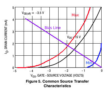
Let’s take a look at the JFET’s characteristic curve:
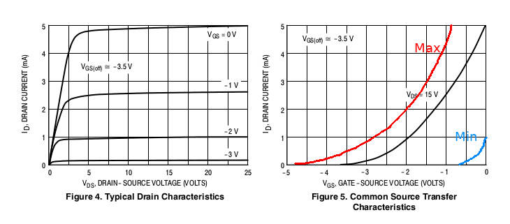
I’ve inserted the minimum and maximum curves for JFET. They correspondant approximately to the minimum and maximum pinch-off voltage of this particular JFET, the 2N5457. As we can see, there is a lot variability: our JFET’s curve can be anywhere in between these two limit curves. Most notably, there is a great range of possibility of the pinch off voltage, or  , and the drain saturation current
  .
.
Thankfully, proper biasing of our JFET can greatly decrease the effects of JFET variability. Let’s take a look at the three JFET biasing methods and how they compare.
Gate Biais
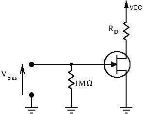
This is the most straightforward. We simply connect a fixed (negative) voltage source at the gate and ground the source. To get the bias voltage, we need to do a DC analysis, which means the AC input is grounded. With this DC-analysis, we can see that  is constant, equal to
  and does not change. Let’s draw our conclusion on the JFET’s characteristic curves:
We want our drain current  to have the greatest swing possible. With gate bias, this swing is heavily dependent on the JFET. If we’re lucky, the JFET’s specific curve will land nicely where we want it to. However, if we’re unlucky, our JFET will not respond at all to our biasing (look at the blue curve!). Because this type of biasing requires us to find a proper JFET before this circuit can work, it is not optimal for circuit design.
Self Bias
Once again, let’s find with a DC analysis, ignoring the input voltage  . Here,
  provides a voltage drop from source to ground, which means that the source is no longer at ground. This changes :
![\[ V_{GS} = V_G - V_S = 0 - R_S \times I_D = -R_S I_D \]](http://modernhamguy.com/wp-content/ql-cache/quicklatex.com-31ce39dbd20e9e6339633666ff8cd7fe_l3.png "Rendered by QuickLaTeX.com")
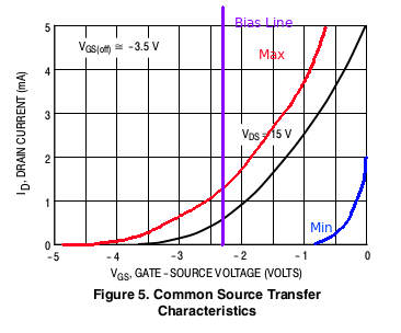
We can trace our bias line on the characteristic curves. We just need two points:
 gives
gives 
 gives
gives 
This is already much better! Our bias line crosses every possible characteristic curves. If we use this kind of biasing, we are certain that our circuit will react. However, for extreme cases (our limit curves), we still limit the possible spread of .
This biasing method is very simple, works well, and is thus very commonly used.
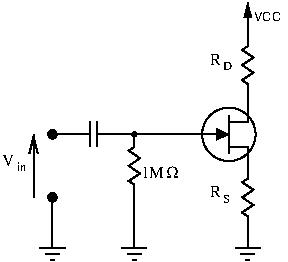
Voltage Divider Bias
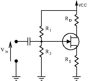
Let’s find  :
:
A simple voltage divider formula gives us  :
:
![\[ V_G = V_{CC} \times \frac{R_2}{R_1 + R_2} \]](http://modernhamguy.com/wp-content/ql-cache/quicklatex.com-d2c936a546004b0efaeb2957e3b5133f_l3.png "Rendered by QuickLaTeX.com")
![\[ Ohm's law can give us $V_S$: V_S = R_S I_D \]](http://modernhamguy.com/wp-content/ql-cache/quicklatex.com-614db925b1b0e689d1bf961047c98fc5_l3.png "Rendered by QuickLaTeX.com")
All together now:
![\[ V_{GS} = V_{CC} \times \frac{R_2}{R_1 + R_2} - R_S I_D \]](http://modernhamguy.com/wp-content/ql-cache/quicklatex.com-153faef63f6e213a266d280178622e00_l3.png "Rendered by QuickLaTeX.com")
Let’s trace this over our characteristic curves:
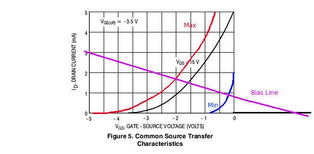
Much better! See how our bias line crosses each and every curve at roughly the same point? This method is the most immune to JFET variability.
Conclusion
While voltage divider bias is clearly the best biasing method for JFETs if we want to diminish JFET variability, sometimes the added complexity is not worth it. In fact, in most JFET circuits you will come across, you will probably see self-bias the most. Both are acceptable, as they both save us from having to cherry pick components.
In the next chapters we will focus our attention on the three classical JFET amplifier circuits.