Introduction
Just like bipolar junction transistors, we also have three classical amplifier configurations for JFET that lay the foundation for all JFET amplifier theory. They are the Common Source amplifier, the Common Drain amplifier, and the Common Gate amplifier. In this chapter we’ll discuss the Common Source amplifier.
JFET Particulars
Let’s recall the small signal equivalent circuit for our JFET:
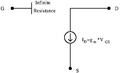
Contrary to our BJT circuits, there is no current flowing into the gate: there is an open circuit after the gate. As we will see later, this will greatly increase our input resistance. Furthermore, no current flowing into the gate means that biasing is voltage only, and doesn’t consume power.
The Common Source Amplifier
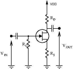
The above schematic represents the common source amplifier: the input is applied at the gate, while the output is sampled at the drain. It is very similar to the common emitter amplifier, where input was applied at the base and output sampled at the collector. In this circuit, self-bias was used as the biasing method.
Just as we did for the BJT amplifier circuits, for each JFET configuration we will derive the voltage gain, current gain, input resistance, and output resistance.
Voltage Gain
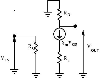
Let’s draw our small signal equivalent circuit:
Remember that the current flowing through the Drain-Source junction is  . It is important to note that our input voltage is not
  , but only
  :
:


But, calculating the ration  doesn’t give a meaningful answer. But what else do we know? Let’s take look more closely at :
![\[ v_{GS} = v_G - v_S = v_{in} - R_S I_D \]](http://modernhamguy.com/wp-content/ql-cache/quicklatex.com-3f4c83285a7ef72af328da91d12d54cc_l3.png "Rendered by QuickLaTeX.com")
![\[ v_{in} = v_{GS} + R_S I_D \]](http://modernhamguy.com/wp-content/ql-cache/quicklatex.com-8b1fc70fda8bf3784453c1cc1fde55eb_l3.png "Rendered by QuickLaTeX.com")
![\[ v_{in} = v_{GS} + R_S g_m v_{GS} \]](http://modernhamguy.com/wp-content/ql-cache/quicklatex.com-9dec3b0ffbaf1e70b1db67c50b9566a9_l3.png "Rendered by QuickLaTeX.com")
(1) 
Now we’re getting somewhere! We can derive our voltage gain  :
:
![\[ \frac{v_{out}}{v_{in}} = \frac{V_{CC} - R_D I_D}{v_{GS} (1+R_S g_m)} \]](http://modernhamguy.com/wp-content/ql-cache/quicklatex.com-c5da8390395d1de41e4df967210d9785_l3.png "Rendered by QuickLaTeX.com")
![\[ \frac{v_{out}}{v_{in}} = \frac{V_{CC} - R_D g_m v_{GS}}{v_{GS}(1+R_S g_m)} \]](http://modernhamguy.com/wp-content/ql-cache/quicklatex.com-2f0ed61662859fff836bd446b1ae4931_l3.png "Rendered by QuickLaTeX.com")
To get the gain, we simply differentiate this result:
![\[ A_v = \frac{\Delta v_{out}}{\Delta v_{in}} = \frac{-R_D g_m v_{GS}}{v_{GS}(1+R_S g_m)} = -\frac{R_D g_m}{1 + R_S g_m} \]](http://modernhamguy.com/wp-content/ql-cache/quicklatex.com-eaeede6dd7d30f3ff97148573e343a31_l3.png "Rendered by QuickLaTeX.com")
![\[ A_v \approx - \frac{R_D}{R_S} \]](http://modernhamguy.com/wp-content/ql-cache/quicklatex.com-0aeb74f437411fb426bb167dc9cf07a9_l3.png "Rendered by QuickLaTeX.com")
The voltage is negative, so the common source amplifier is an inverting amplifier. However, the schematic I’ve shown you is not really a common source amplifier. Indeed, the source isn’t AC-grounded. Let’s change that and add a bypass capacitor on the source:

The small signal equivalent circuit is:
In which case, we have :

 (the source is AC grounded)
This gives us a voltage gain of  .
.
If we add a load  to our circuit, this gain changes and becomes
  .
.
Source Degeneration
So, we have a voltage gain. There is a small problem however: the gain is heavily dependent on  , and in the case of JFETs, can vary widely from on transistor to the next. Just like the common emitter amplifier, we can reduce the effect of variability by introducing a source resistor: this is called source degeneration.

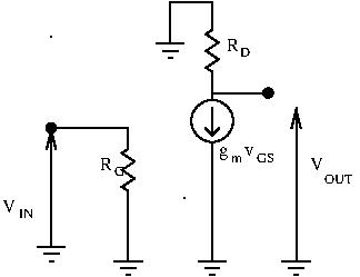
The small signal equivalent circuit is:

Let’s calculate the new voltage gain:

We can express  as a function of
  :
: 
Now we can derive our voltage gain :
![\[ A_v = \frac{\Delta v_{OUT}}{\Delta v_{IN}} = \frac{-R_D g_m v_{GS}}{v_{GS}(1 +R_{S1} g_m)} = -\frac{R_D g_m}{1 + R_{S1} g_m} \]](http://modernhamguy.com/wp-content/ql-cache/quicklatex.com-dd22d4d17427f114ef48c58c0a46523a_l3.png "Rendered by QuickLaTeX.com")
![\[ A_v \approx -\frac{R_D}{\frac{1}{g_m} + R_{S1}} \]](http://modernhamguy.com/wp-content/ql-cache/quicklatex.com-10283a74dce3eaf09ba36c1da4af16bb_l3.png "Rendered by QuickLaTeX.com")
To effectively use source degeneration, choose  high enough to swamp
  , but not too large as to kill the gain. Doing so, we can ignore and the gain will be approximately
  .
.
Current Gain
As we saw earlier, there is no current flowing through the gate of our JFET. This means that no current from our input signal can flow into our amplifier. This circuit draws no current, but still delivers current. The current gain is infinite.
Input Resistance
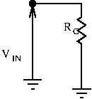
There is an open circuit at the gate. The only path the input signal can take is through  . Technically, isn’t required, but it is good practice to include it. This way, if something goes wrong with your input signal (ground problems, etc), there is a path to ground for the gate, allowing the transistor to fully ‘deactivate’ and avoid damage. In the absence of an input signal, the gate is grounded and not floating.
Back to our input resistance. Following the above circuit, it is trivially  . We choose to be generally in the hundreds of k
 or in the megaohm range.
We see here one big advantage of JFET’s over BJTs: they have incredibly high input resistances. If we are using voltage dividers for biasing the gate, since there is no biasing current, there is no need for a stiff voltage source: you can use very high value resistors and greatly reduce the current draw of your biasing network.

Output Resistance
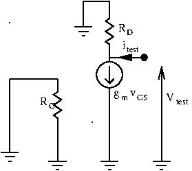
To calculate the output resistance the academic way, we need to ground the input, and apply a test signal at the output  , and calculate the ratio
  .
.
![\[ i_{test} = \frac{v_{test}}{R_D} + g_m v_{GS} \]](http://modernhamguy.com/wp-content/ql-cache/quicklatex.com-5ac42d849292908201ee987978bd2c60_l3.png "Rendered by QuickLaTeX.com")
Lets explicit :
![\[ v_{GS} = v_G - V_S \]](http://modernhamguy.com/wp-content/ql-cache/quicklatex.com-e09acdc0df5011498844d8daf3624dbe_l3.png "Rendered by QuickLaTeX.com")
However, we know the input is grounded, so  , and the source is also AC-grounded by the bypass capacitor. This gives us
  , and thus
  . The output resistance is then simply:
![\[ R_{OUT} = \frac{v_{test}}{i_{test}} = \frac{v_{test}}{v_{test} R_D}} = R_D \]](http://modernhamguy.com/wp-content/ql-cache/quicklatex.com-77fc192f629ee968a3ccf8386afe14d1_l3.png "Rendered by QuickLaTeX.com")

This is usually moderately high.
Conclusion
Let’s recap what we’ve learned on the common source amplifier:
 (if no source degeneration)
 is infinite
- , very high
 , moderately high