When studying amplifiers it’s impossible to leave out the differential amplifier. It is a very common and well known building block in electronics, and is also the basis for one of the most popular RF mixers: the Gilbert Cell mixers. Learning about the differential amplifier won’t just give you a useful tool in your electronic repertoire, but it also gives us a good excuse to introduce what CMRR – Common Mode Rejection Ratio- is.
Differential amplifiers can be easily made with a single op-amp. Some op-amps are even specifically designed to be used as such and don’t require external circuitry. In this article however, we’re going to focus on the transistor differential amplifier.
Transistor Differential Amplifier

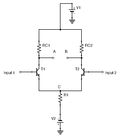
Note here that we have two possible inputs: one for each transistor’s base. We also have two possible outputs: one for each transistor’s collector. We can use this amplifier configuration in multiple ways:
- using only one input: this is called single-ended input
- using both inputs: this is called differential input
- using one output: this is called single-ended output
- using both outputs: this is called differential output
When using differential amplifiers, two different gains can be calculated: the differential gain, and the common-mode gain.
The differential gain is determined with a differential input signal, while the common-mode gain is determined with the same signal applied at both inputs.
Let’s start with the common-mode gain.
Common-Mode Gain

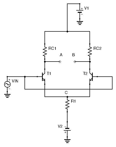
Let’s apply an identical signal to both inputs. The two transistors are identical, and both collector resistors are identical. Therefore, since the same signal is applied to both transistors, the same current flows through them both. At point A, the two identical currents flowing from both transistors flow into the common emitter resistor ![]() . A common mistake would be to assume that the gain of this circuit is simply
. A common mistake would be to assume that the gain of this circuit is simply ![]() . The reason this is not correct is because the common emitter resistor
. The reason this is not correct is because the common emitter resistor ![]() sees twice the current that either transistor handles. So how do we find the true gain of this circuit? A neat little trick outlined in The Art of Electronics simplifies this process nicely. First, replace
sees twice the current that either transistor handles. So how do we find the true gain of this circuit? A neat little trick outlined in The Art of Electronics simplifies this process nicely. First, replace ![]() by an equivalent resistor network consisting of two
by an equivalent resistor network consisting of two ![]() resistors in parallel, like so:
resistors in parallel, like so:

Now, we know that the transistor currents don’t flow from one transistor to the other, but instead go through the common emitter resistor(s). Therefore, opening the circuit at point C is of no consequence. Indeed, both legs of the differential amplifier handle the same current, and the same current will flow through each ![]() resistor:
resistor:

We can now easily find the gain. Each transistor is in a classic common emitter configuration, so gain is ![]() . Our common-mode gain is thus:
. Our common-mode gain is thus:
![]()
The output is identical regardless of which output point A or B is used. Taking the differential output (![]() ) will yield zero. In practical circuits the differential output will always show some minute voltages due the transistors not being perfectly matched, and due to the resistors’ tolerances.
) will yield zero. In practical circuits the differential output will always show some minute voltages due the transistors not being perfectly matched, and due to the resistors’ tolerances.
Differential Gain
To find the differential gain, instead of applying the same signal to both inputs, we apply a differential input, as follows:

Here, ![]() .
.
A little math is required to find this circuit’s gain. Using the transistor’s equivalent circuit (see here for more details), we know that each collector’s current is:
![]()
Our output voltage is thus:
![]()
With ![]() , with
, with ![]() in mA. Now we need to express v_{BE} as a function of our input signal
in mA. Now we need to express v_{BE} as a function of our input signal ![]() For each transistor however,
For each transistor however, ![]() is different:
is different:
- Left transistor:

- Right transistor:

To find the gain here, we need to realize one important characteristic of this circuit. The input is differential. That means that for every 1mV of signal increase at transistor ![]() ‘s base, there is an equal and opposite 1mV of signal decrease at transistor
‘s base, there is an equal and opposite 1mV of signal decrease at transistor ![]() ‘s base. Since the transistors and collector resistors are identical, this means that when collector voltage drops by a certain amount at
‘s base. Since the transistors and collector resistors are identical, this means that when collector voltage drops by a certain amount at ![]() , then the collector voltage at
, then the collector voltage at ![]() increases by the same amount. The same can be said for their emitter voltage. Since both emitters are connected at point A, point A is a fixed voltage that doesn’t change with the input signal.
increases by the same amount. The same can be said for their emitter voltage. Since both emitters are connected at point A, point A is a fixed voltage that doesn’t change with the input signal. ![]() is a constant.
is a constant.
The last thing we need to understand is the relationship between ![]() ,
, ![]() , and
, and ![]() . For every mV of increase in
. For every mV of increase in ![]() ,
, ![]() decreases by the same amount. This causes
decreases by the same amount. This causes ![]() to change by twice that amount. Another way to see it is that for every increase in 1mV of
to change by twice that amount. Another way to see it is that for every increase in 1mV of ![]() ,
, ![]() increases by 0.5mV and
increases by 0.5mV and ![]() decreases by 0.5mV.
decreases by 0.5mV.
![]()
![]()
Here, ![]() is either
is either ![]() or
or ![]() depending on which transistor we choose:
depending on which transistor we choose:
- for
 :
: 
- for
 :
: 
With the reasoning of the previous paragraph we can now link ![]() and
and ![]() with
with ![]() :
:
- for
 :
: 
- for
 :
: 
And thus, we have:
![]()
If used as a single-ended output amplifier, this configuration, depending on which collector we sample our output voltage, will either have positive or negative gain.
However, if used as a double-ended output amplifier, as shown below, the gain changes.
In this case:
![]()
![]()
Thus, the gain becomes!
![]()
Which is twice the gain of the single-ended output configuration.
To increase thermal stability and stabilize gain, identical emitter resistors can be used before point A.
CMRR – Common Mode Rejection Ratio
We’ve covered what Common Mode signals were: this is when both inputs are identical. In the case of the differential amplifier, when using a common mode input, the differential output is nil. This means that this circuit can get rid of parasitic offsets that are common to both inputs. An differential amplifier can thus clean up a noisy signal, up to a point.
An amplifier’s capability of eliminating common mode signals is measured by its CMRR: its common mode rejection ratio. Mathematically speaking, CMRR is equal to the ratio of differential gain over common mode gain, often expressed in dB
![]()
An ideal differential amplifier would have an infinite CMRR. For the differential amplifier studied in this article, we can calculate the theoretical CMRR:
![]()
Since ![]() , we have:
, we have:
![]()
Conclusion
I hope this article made differential amplifiers clearer for you. We’ll be seeing them again, most notably when we’ll be studying Gilbert Cell mixers. While we only focused on the BJT differential amplifier here, a differential amplifier can be built with FETs and Op-Amps as well.