Introduction
So far, we have studied BJTs and their different configurations, isolated from any other circuitry. We’ve learned a lot, and we’re much further along than we first started. However, until now we haven’t given much thought as to our circuit’s frequency response, and how differently that can behave depending on our input signal’s frequency.
High Frequency Models
If we stick to our low-frequency transistor model, we won’t see anything particularly worrisome when increasing our input frequency. But that model doesn’t give us the whole picture, even if it is an acceptable approximation for lower frequency signals. For RF design however, this model isn’t enough, and we’ll need to introduce the transistor’s imperfections into the mix to appropriately predict a circuit’s behavior at higher frequencies. Let’s take a closer look at our bipolar junction transistor:
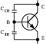
In reality, you have parasitic capacitance’s between Base and Emitter, and between Base and Collector. This is not intentional, but rather an unavoidable artifact from the manufacturing process. A simple way to understand this parasitic capacitance is to look back at our PN junction.
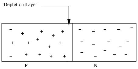
There is an accumulation of charge at this junction, and thus this junction exhibits capacitance. We have 2 PN junctions in BJT, so we have 2 parasitic capacitance’s. They are very low, on the order of a few picofarads. Remember that a capacitor’s impedance is  . At low frequencies,
  is very low, so this parasitic capacitance can be safely ignored. At higher frequencies however, they can start altering our circuit’s behavior. To better quantify this effect, let’s introduce the transistor’s high-frequency model, also called the hybrid-pi model:
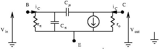
In the above model,  . Let’s apply an input signal and try to determine the current gain of the amplifier. We want to see if it still
  . Let’s find an expression for
  and
and  and find the ratio.
For  , we short the collector output and find:
![\[ i_B = \frac{v_{in}}{r_\pi} + \frac{v_{in}}{Z_C_\pi} + \frac{v_{in}}{Z_C_\mu} \]](http://modernhamguy.com/wp-content/ql-cache/quicklatex.com-c699132690e1d69be5df6bca3596d95c_l3.png "Rendered by QuickLaTeX.com")
![\[ i_b = v_{in} \times (\frac{1}{r_\pi} + \frac{1}{Z_C_\pi} + \frac{1}{Z_C_\mu}) \]](http://modernhamguy.com/wp-content/ql-cache/quicklatex.com-d5f20b057db66176eecd93779b833e94_l3.png "Rendered by QuickLaTeX.com")
![\[ i_b = v_{in} \times (\frac{1}{r_\pi} + j\omega(C_\pi + C_\mu)) \]](http://modernhamguy.com/wp-content/ql-cache/quicklatex.com-39f770c30af2abdc3f929a98b7e72f94_l3.png "Rendered by QuickLaTeX.com")
And now for  , we find:
![\[ i_C = g_m v_{in} - \frac{v_{in}}{Z_C_\mu} \]](http://modernhamguy.com/wp-content/ql-cache/quicklatex.com-2dffca48d5b0c77ecf7d83441e2d3c36_l3.png "Rendered by QuickLaTeX.com")
![\[ i_C = g_m v_{in} - jC_\mu \omega v_{in} \]](http://modernhamguy.com/wp-content/ql-cache/quicklatex.com-063590929b392857f51f1a6ce4c3f3ce_l3.png "Rendered by QuickLaTeX.com")
![\[ i_C = v_{in} (g_m - jC_\mu \omega) \]](http://modernhamguy.com/wp-content/ql-cache/quicklatex.com-6c061ef53e39cdc4d8c2bb5dd6c660f9_l3.png "Rendered by QuickLaTeX.com")
We can now derive our current gain  :
:
![\[ A_i = \frac{i_c}{i_b} = \frac{g_m - jC_\mu \omega}{\frac{1}{r_\pi} + j\omega (C_\pi + C_\mu)} \]](http://modernhamguy.com/wp-content/ql-cache/quicklatex.com-0eab25f11dba18b907f389cce00ecb79_l3.png "Rendered by QuickLaTeX.com")
![\[ A_i = \frac{r_\pi g_m - r_\pi j C_\mu \omega}{1 + j r_\pi \omega (C_\pi + C_\mu)} \]](http://modernhamguy.com/wp-content/ql-cache/quicklatex.com-bb2ac15f4d537d13728c55f23bcc800c_l3.png "Rendered by QuickLaTeX.com")
To make sense of this equation, let’s give some actual numbers for these values:


Knowing this, we can simplify our above equation:
![\[ A_i = \frac{r_\pi g_m}{1 + jr_\pi \omega (C_\pi + C_\mu)} \]](http://modernhamguy.com/wp-content/ql-cache/quicklatex.com-2e5bda9afc4dd4a86b7dc4dc7bf373e0_l3.png "Rendered by QuickLaTeX.com")
We can simplify this equation further by remembering that  .
.
So, our current gain becomes:
(1) 
Note that our current gain is frequency-dependant!
If you’ve studied a little bit of control theory, you’ll recognize a first order transfer function:
![\[ h(\omega) = \frac{\beta}{1 + j\frac{\omega}{\omega_0}} \]](http://modernhamguy.com/wp-content/ql-cache/quicklatex.com-34e03df592d621feeaf0d8b3866442d8_l3.png "Rendered by QuickLaTeX.com")
with 
We can define a bandwidth  . BJTs have bandwidth! We can also get the transistor’s current gain depending on the signal frequency:
- for low frequencies:

- for high frequencies:

So
An important characteristic of a transistor is its gain-bandwidth product  . It represents the frequency at which gain is unity. Here, gain is unity when
  .
.
We can express the high frequency current gain with the following equation:
![\[ h(\omega) \approx \frac{\omega_{BP}}{\omega} \]](http://modernhamguy.com/wp-content/ql-cache/quicklatex.com-18ea2d98ad2137bca7a4ccde3f5a7654_l3.png "Rendered by QuickLaTeX.com")
The gain-bandwidth product is a fundamental characteristic for higher frequency circuits, and is available in every datasheet.
Altered Circuit Behavior at Higher Frequencies
With that out of the way, let’s see how these extra capacitance’s can hinder our designs. We’ve seen that our current gain decreases with frequency, but we’re still able to have huge bandwidth right? The gain-bandwidth product for the common 2N3904 NPN transistor gives us  (remember
  ). This is the frequency at which our current gain is unity (the transistor can no longer amplify). So, if we want to have a gain of say, 50, then our bandwidth would be
  . Unfortunately, it isn’t that simple, and depending on how we exploit our transistors, we can end up having a drastically lower bandwidth.
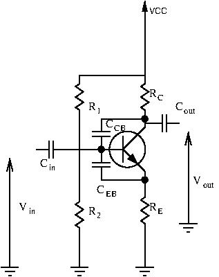
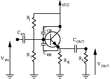
Let’s take a look at our CE amplifier again, this time adding  and
and  :
:
For a capacitor: 
So here,  (remember that the CE amplifier is an inverting amplifier.
Let’s inject this into our capacitor charge formula:
![\[ Q_{CB} = C_{CB} (A_v +1) V_{IN} \]](http://modernhamguy.com/wp-content/ql-cache/quicklatex.com-b1a2833831451239eb46a0dce39f06e4_l3.png "Rendered by QuickLaTeX.com")
Notice that in this equation an apparent capacitance  appears. The voltage drop across CB increases the apparent capacitance and hinders high frequency performance. Bandwidth is reduced by a factor of
  . This is the Miller Effect. Keep in mind that
  doesn’t change, but that with high voltage drop its acts like a
  times bigger capacitance.
The Miller Effect in Other Circuits
Not all transistor amplifier configurations suffer from this effect. To understand why, let’s do the calculations for the CB amplifier and the CC amplifier.
Here we have:
![\[ Q_{CB} = C_{CB} V_{CB} \]](http://modernhamguy.com/wp-content/ql-cache/quicklatex.com-37a24a01b720d423949a6978499f8cf1_l3.png "Rendered by QuickLaTeX.com")
![\[ Q_{CB} = C_{CB} (V_{OUT} - V_{IN}) \]](http://modernhamguy.com/wp-content/ql-cache/quicklatex.com-07ade2f62ba7061ec53c4545f6fe8d47_l3.png "Rendered by QuickLaTeX.com")
Since there is very little voltage drop between  and
and  :
:
![\[ Q_{CB} \approx 0 \]](http://modernhamguy.com/wp-content/ql-cache/quicklatex.com-95fd7f4a9bf88ff8603d7d0892b785ae_l3.png "Rendered by QuickLaTeX.com")
No Miller Effect for the CC amplifier. There is very little voltage drop between collector and base.
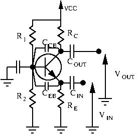
For the CB amplifier:
![\[ Q_{CB} = C_{CB} (V_{OUT} - 0}) \]](http://modernhamguy.com/wp-content/ql-cache/quicklatex.com-4b9c32767fd98aec1866f6c5f50c21d3_l3.png "Rendered by QuickLaTeX.com")
![\[ Q_{CB} = C_{CB} V_{OUT} \]](http://modernhamguy.com/wp-content/ql-cache/quicklatex.com-f0aa31713f6f01b2450d33b6691aa8ec_l3.png "Rendered by QuickLaTeX.com")
The base is grounded, there is no Miller Effect.
Conclusion:
Out of the three BJT amplifier configurations, only the CE amplifier suffers from the Miller Effect. However, this doesn’t mean we’re limited to CC and CB amplifiers for HF work. CE amplifiers CAN be used for high frequency circuits, you just need to be mindful of the limitations, and that your bandwidth will be restricted.
The Miller Effect doesn’t apply to just BJT amplifiers. All inverting amplifiers suffer from it.
To get around the Miller Effect, a special configuration can be used. In the next chapter we’ll talk about the cascode amplifier.