Introduction
Our next classic configuration is the Common Collector, or CC amplifier. We’ve already covered AC-coupling and biasing in the previous chapter on the CE amplifier. The concept is the same here and won’t be detailed. For the CC amplifier, we’ll learn how to
- Draw the DC and AC load lines
- Get the voltage and current gain
- Derive the input and output resistance
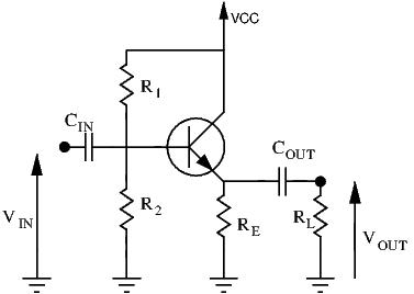
In this configuration, input is still applied at the base, while the output is sampled at the emitter. To analyse this circuit, let’s draw the small signal equivalent circuit:
DC and AC Load Lines
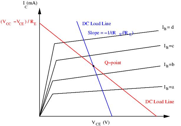
Find the load lines is essential for determining whether or not our Q-point, and thus our biasing, is adequate or not. The DC load line can be found using the original circuit and using KVL on the loop going from  to ground. This gives us the following equation:
![\[ V_{CC} - R_E \times I_E - V_{CE}= 0 \]](http://modernhamguy.com/wp-content/ql-cache/quicklatex.com-9505eefd0cc4b696865e1788e47914b3_l3.png "Rendered by QuickLaTeX.com")
We can safely say that  . By substituting in the above equation, we have the obtain the following:
![\[ I_C = \frac{V_{CC}-V_{CE}}{R_E} \]](http://modernhamguy.com/wp-content/ql-cache/quicklatex.com-5545afa09475e37d9c2878ca0001b42a_l3.png "Rendered by QuickLaTeX.com")
Using the DC load line, we can plot our Q-point on the characteristic curves of the transistor.
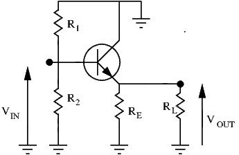
By adding the load and using the small signal equivalent circuit, we can apply KVL on the loop going from ground to ground, giving us the following equation:
![\[ 0 - v_{CE} - (R_E // R_L) \times i_E = 0 \]](http://modernhamguy.com/wp-content/ql-cache/quicklatex.com-27d0c3f4e60aa58aa6ffc4fdc2104f7d_l3.png "Rendered by QuickLaTeX.com")
Substituting  for
for  , we obtain:
![\[ i_E = - \frac{v_{CE} }{R_E // R_L} \]](http://modernhamguy.com/wp-content/ql-cache/quicklatex.com-a2ad2226286bba00d8094323bdac5e0f_l3.png "Rendered by QuickLaTeX.com")
We can now plot our DC and AC load lines on our characteristic curves:
Voltage Gain
Voltage gain for the CC amplifier is quite straightforward. For an NPN transistor, recall that  . The input signal is applied at the base, so
  . The output is sampled at the collector, so the output voltage is
  . Quite simply:
![\[ v_E = v_B - 0.7 V \]](http://modernhamguy.com/wp-content/ql-cache/quicklatex.com-025285dddd21731a42bd50d018583a96_l3.png "Rendered by QuickLaTeX.com")
Or put in other terms:
![\[ v_{OUT} = v_{IN} - 0.7 V \]](http://modernhamguy.com/wp-content/ql-cache/quicklatex.com-84a2fd9cd0095c224ff45ad7fc281879_l3.png "Rendered by QuickLaTeX.com")
As we can see, the output voltage is only a diode voltage drop away from the input voltage: they are nearly equal:  . This gives a voltage gain
  a little less than unity:
  . By this point, some of you may be wondering why we would bother with this configuration if we want to make an amplifier. So far, the only thing the CC amplifier does is replicate the input signal (with a small voltage drop). Now, while it’s true that this amplifier has no voltage gain, it does have a current gain of
  ! As RF enthusiasts, what interests us the most is not voltage or current gain, but power gain. And with a high current gain of (around 100-300), our CC amplifier definitely has power gain, even without any voltage gain.
By looking at the input and output resistances, we’ll find out why this amplifier configuration has a very useful characteristic and is a building block in many radio and audio circuits.
Input Resistance
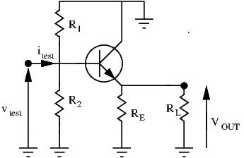
As usual, we calculate the input resistance by applying a test voltage at the input and determining the test current delivered into the circuit. By following the red line, we have  . A the emitter node E, two currents merge to flow into
  : the one given by the input signal
  , and the one given by the dependent source
  . Let’s derive :
(1) 
Alright, now let’s express  as a function of . First, let’s calculate :
![\[ v_E = (R_E // R_L) \times (i_b + \beta \times i_b) = (R_E // R_L) \times (\beta +1) \times i_b \]](http://modernhamguy.com/wp-content/ql-cache/quicklatex.com-ef25f8062ae452edfaf202d8f68d5e80_l3.png "Rendered by QuickLaTeX.com")
To get , we now just need to know  :
:
![\[ v_{r_e} = i_b \times (\beta + 1) \times r_e \]](http://modernhamguy.com/wp-content/ql-cache/quicklatex.com-ff16741abed523df05805673145bbeac_l3.png "Rendered by QuickLaTeX.com")
Adding and gives us  :
:
![\[ v_{test} = (\beta + 1) \times (R_E // R_L) \times i_b + (\beta + 1) \times r_e \]](http://modernhamguy.com/wp-content/ql-cache/quicklatex.com-992e6bdde5761ddc501e9aa065bff334_l3.png "Rendered by QuickLaTeX.com")
(2) 
Substituting with the help of equation (1), we obtain:
(3) 
This looks like a pretty complex equation, but there is a viable approximation we can make that can largely simplify it.  and
and  are our biasing resistors and are generally quite large (thousands or tens of thousands of ohms) to avoid draining too much current. These two resistor values are (generally) much higher than any other resistances in the amplifier. Thus we can safely say that
  . Equation (3) is greatly simplified by using this approximation:
(4) 
Our input resistance is thus  . This value is relatively high (notice the multiplication). A high
  means this circuit draws very little current from its previous stage, thus not loading it too much.
Output Resistance
Just like for the CE amplifier, finding the output resistance is greatly simplified if we first find the equivalent Thevenin model of the circuit. We’ll follow the same steps as before to find the equivalent model:
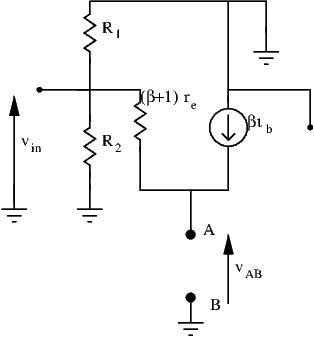
- Let’s remove the load and also
 and fix our two points A and B, as seen above
 - Our open-circuit voltage is simply

- We short AB and get the short circuit current
 :
:

![\[ i_{AB} = i_b + \beta \times i_b \]](http://modernhamguy.com/wp-content/ql-cache/quicklatex.com-2ea9792db73062d8a3bf71f167a80900_l3.png "Rendered by QuickLaTeX.com")
![\[ i_{AB} = \frac{v_{IN}}{ (\beta +1) \times r_e} + \beta \times \frac{v_{in}}{(\beta + 1) \times r_e} = (\beta +1) \times \frac{v_{in}}{(\beta +1) \times r_e} \]](http://modernhamguy.com/wp-content/ql-cache/quicklatex.com-4dc2a575e7d3bc993ca765b544b105c6_l3.png "Rendered by QuickLaTeX.com")
![\[ i_{AB} = \frac{v_{in}}{r_e} \]](http://modernhamguy.com/wp-content/ql-cache/quicklatex.com-8e138ae0c95c760429f6cb2eeb2d80d5_l3.png "Rendered by QuickLaTeX.com")
- We can now find the Thevenin resistance

We can now greatly simplify our CC small signal model by the following:
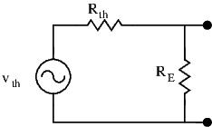
Finding the output resistance is now greatly facilitated: 
SInce r_e is very small (tens of ohms) compared to R_E, we can simplify the equation:
![\[ R_{out} = r_e \]](http://modernhamguy.com/wp-content/ql-cache/quicklatex.com-fbc1a252fec323f4b0fce384e9526d97_l3.png "Rendered by QuickLaTeX.com")
r_e being very small, the CC amplifier has a low output resistance. Low output resistance is ideal for delivering high amounts of current to the load.
Conclusion
Let’s recap what we found out so far:


Unity voltage gain, high input resistance, and low output resistance: these are the characteristics of a buffer circuit. Its role is to isolate different blocks so that they don’t interfere with each other. This circuit can be placed after a stage with high output resistance, such as the CE amplifier from before, to deliver more current without voltage dropping. Buffers are great for exploiting ‘fragile’ circuits with high output resistance whose voltage drop very quickly with load current. Because of its unity voltage gain, the CC amplifier is also called the Emitter Follower.