Introduction:
We will start our study of BJT amplifiers with the Common Emitter amplifier, commonly abbreviated as the CE amplifier. This configuration is probably the most common of all BJT amplifiers, and the one you will see most often, in one form or another, in the ham literature. Understanding the CE amplifier already gives you a powerful reference when analyzing circuits.
Our goal here is to understand what each component in this classical circuit is used for, and what are the characteristics of the amplifier. More specifically, we will derive voltage gain, current gain, input resistance, and output resistance.
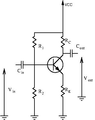
AC Coupling
Let’s take a closer look at the schematic, as there are plenty of interesting things going on here.
First, notice how the input signal  isn’t applied directly to the base, but instead passes through capacitor
  first. Recall that a capacitor acts like a short for AC signals, but like an open circuit for DC. This allows our input signal to pass through the capacitor while stopping DC voltage from our power supply from leaking out. This is called AC coupling the input.
Biasing the Transistor
We know that a transistor requires a power supply to work. Here, this power supply is modeled with  . But what are
  and
and  used for? Wouldn’t the circuit work without them? Well no, or more exactly, not all the time. As we explained in our chapter on BJTs, the Base-Emitter junction of NPN transistors need to be forward biased for the transistor to conduct. Knowing this, if we want our amplifier to amplify signals all the time, the BE junction needs to be forward biased all the time. This means that we must have
  all the time. If we only apply at the base without anything else, then we would have
  . But is a pure AC signal with no DC offset (the capacitor gets rid of any DC offset if present), it will swing between two values, one positive and one negative.
This will cause our transistor to turn off when  . Our output signal will be heavily distorted.
However, if we add some DC offset to the base voltage, such that even with the swing of our input voltage all the time, then we can guarantee that our transistor will be always on. This is called biasing the transistor. There are several methods to do this, but the most common is the one shown in the full schematic. Here, biasing is done with a voltage divider created by and . This gives the transistor a bias voltage approximately equal to:
![\[ V_B = \frac{R_2}{(R_1 + R_2)} \times V_C_C \]](http://modernhamguy.com/wp-content/ql-cache/quicklatex.com-89216dba9ce0132b53eac76451ac7beb_l3.png "Rendered by QuickLaTeX.com")
Why approximately? The voltage divider formula is only valid if no current is lost between the two resistances. Here, not all the current flows through and . Indeed, a small amount of current is sent through the Base-Emitter junction. The formula is thus not valid and will not give the exact bias voltage. However, since the base current is very small, the formula will still give a reasonably accurate value that we can exploit.
The exact voltage chosen for biasing depends on the transistor’s characteristics. We will see how in the following paragraphs.
The Quiescent Point
What is the Q-Point?
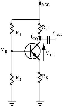
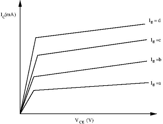
With biasing, even without any input signal the transistor still conducts. There is voltage at the base, and there is current flowing through the transistor. This point of operation is called the quiescent point, or Q-point. The collector current at this point is called the quiescent current  . There is a clear way to graphically exploit this point. Let’s take a look at our transistor’s collector characteristic curves, which gives us the relationship
  . A simplified version of these curves is found below:
Graphical Determination of the Q-Point
Let’s place our quiescent point on these curves. Going back to our schematic, a Kirchoff’s Voltage Law loop from  to ground gives us:
(1) 
We can approximate  . Indeed, since
  , with
  , this approximation is accurate enough. Remember that
  , with common values of
  being in the 100-300 range.
With this approximation, equation (1) becomes:
![\[ V_{CC} - (R_C + R_E) \times I_C = V_{CE} \]](http://modernhamguy.com/wp-content/ql-cache/quicklatex.com-0f9b1054fcbb977c053781745260fbb0_l3.png "Rendered by QuickLaTeX.com")
This gives us  :
:
![\[ I_C = V_{CC} - \frac{V{CE}}{R_C + R_E} \]](http://modernhamguy.com/wp-content/ql-cache/quicklatex.com-6b1dad9ec871e78dd85c26f515461fda_l3.png "Rendered by QuickLaTeX.com")
(2) 
Equation (2) gives us a linear equation linking and  . We can plot this straight line on the above transistor characteristic curves. Two points are enough for us to plot it:
 gives us
- When the transistor is fully on,
 gives us
We can now plot this line over the transistor characteristic curves:

Our quiescent point, or Q-point, is somewhere along this slope. We now need to find out which curve we need to use. To select the correct curve, we need to calculate the base current at the quiescent point  .
.
We already calculate  previously with the voltage divider formula:
![\[ V_B = \frac{R_2}{R_1 + R_2} \times V_C_C \]](http://modernhamguy.com/wp-content/ql-cache/quicklatex.com-e2fb8d4abff80663a6bf340e510ae6ca_l3.png "Rendered by QuickLaTeX.com")
We know that if the transistor is on, then  . So if we know , we can derive
  :
:
![\[ V_E = V_B - 0.7 V \]](http://modernhamguy.com/wp-content/ql-cache/quicklatex.com-c3001eb7a3766c04424f4a0f3df1abdb_l3.png "Rendered by QuickLaTeX.com")
Now that V_E is known, finding the emitter current is easy:
![\[ I_E = \frac{V_E}{R_E} \]](http://modernhamguy.com/wp-content/ql-cache/quicklatex.com-654f28ff6a79364997f5543596f6a88f_l3.png "Rendered by QuickLaTeX.com")
We’ve already established that we can approximate  , and since , we have:
![\[ I_B = \frac{V_B - 0.7 V}{\beta \times R_E} \]](http://modernhamguy.com/wp-content/ql-cache/quicklatex.com-bba96c46a2987d092ee2b8cf5e3c11a1_l3.png "Rendered by QuickLaTeX.com")
Now that we have  , we can select the correct curve on the previous chart. The quiescent base current you will end up finding will very likely not end up corresponding exactly to the set values the characteristic curves are drawn for. In this case, you can simply extrapolate and draw the curve yourself, using the other curves as reference.
The intersection of the slope and the correct characteristic curve gives you the Q-point.
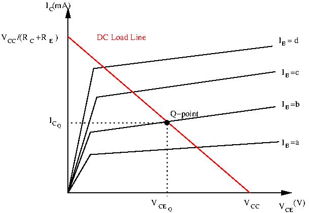
By choosing  and
and  , we limit the possibilities of the amplifier. It’s operation is limited to the load line mentioned above. With no input signal:
  and
and  . This slope is called the DC load line of the amplifier, and depends only on and .
Numerical Determination of the Q-point
You can also find the Q-point by calculation. A KVL loop from  to ground gives us:
![\[ V_{CC} - R_C \times I_C - V_{CE} - R_E \times I_E = 0 \]](http://modernhamguy.com/wp-content/ql-cache/quicklatex.com-c8b8ac9b77e61ac08cbabdf0c21e9a2b_l3.png "Rendered by QuickLaTeX.com")
![\[ V_{CC} -(R_C + R_E) \times I_{CQ} = V_{CEQ} \]](http://modernhamguy.com/wp-content/ql-cache/quicklatex.com-050caea877f04568b9c8567bebcb58b2_l3.png "Rendered by QuickLaTeX.com")
How to Choose the Q-Point?
Notice the shape of the characteristic curves. For very low values of and for high values of (not shown on the graphs, but for high values of,  shoots up and no longer linearly follows ) the shape of the curve changes drastically: the device is in its non-linear region. Operation in this area will give us a heavily distorted output waveform. Instead, we must choose our Q-Point to avoid these areas as much as possible.
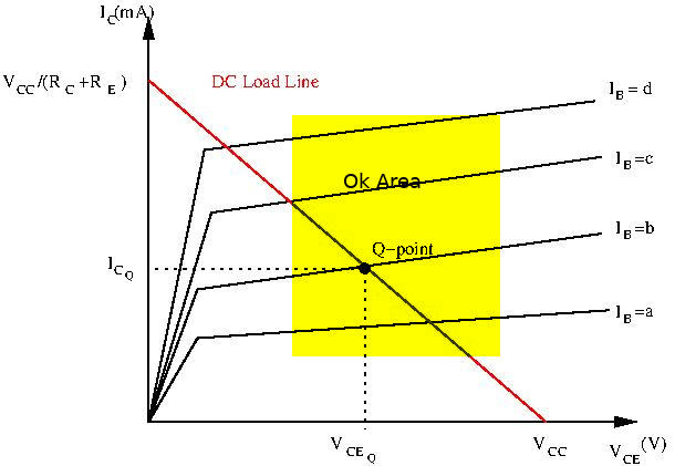
Don’t forget that we will be eventually be applying an input signal at the base. We want to bias the transistor for maximum swing. More about this in the following paragraphs.
Recap
This was a lot to take in, but I wanted to detail all the steps as much as possible. To summarize, to find the Q-Point simply follow the following steps:
- Find the quiescent base voltage
 with the voltage divider formula
 - Find the emitter voltage

- Find the quiescent collector current

- Derive the quiescent base voltage

- Find the Q-Point either graphically, with the DC load line and , or numerically with the KVL loop.
AC Performance
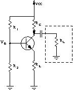
Let’s now add a load at the output of our circuit. our amp is going to power something after all.
Just like  ,
,  allows AC signals to pass through to the load while blocking DC. We seldom want DC offset at the output, but if we do you can simply remove
  . The output here is AC-coupled.
So far we have only studied the DC performance of our amplifier. However, AC signals behave very differently from DC: they way they “see” different circuit elements changes. Furthermore, AC performance of an amplifier is of particular interest to us, as the signals we will be applying to our amplifier will be AC signals. In order to study the AC characteristics of of our amplifier, we need to see the circuit the same way AC signals do: we need to do an AC analysis, or small-signal analysis of our circuit.
This is actually very simple to do. We need to:
- Ground all voltage sources. AC signals view constant voltage sources as ground.
- Open circuit all current sources.
- Replace all capacitors with a short.
- Replace all inductors with an open circuit
If we apply these transformations to our current circuit, we are left with:
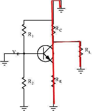
The base is grounded because for now no input signal is applied. Notice now how some current now flows through and  .
.
KVL still applies. From ground to ground we obtain the following KVL equation:
![\[ R_C // R_L \times i_c + i_c \times R_E + V_{CE} = 0 \]](http://modernhamguy.com/wp-content/ql-cache/quicklatex.com-cfde231e1272e1a438253ec2e119ece2_l3.png "Rendered by QuickLaTeX.com")
![\[ i_C = \frac{V_{CE}}{R_E + R_E//R_L} \]](http://modernhamguy.com/wp-content/ql-cache/quicklatex.com-27b930193b2581deecf0d09ec9da92f6_l3.png "Rendered by QuickLaTeX.com")
We can now trace our new AC load line. We only have a slope, here equal to  , but that is enough to draw our load line. We only need one point. We know that without any AC input signal, the transistor is at its Q-Point. So our AC load line must pass through our Q-Point. Knowing this, we can draw our AC load line.

A few words on this AC load line. When an AC signal is applied at the input of our amplifier. The point of operation of our amplifier will swing around our Q-Point along this AC load line. This is more or less true. The AC load line is the limit from which the circuit can stray from its DC operation region. It represents the amplifier’s load line at infinite frequency. In reality, inductors aren’t exactly open circuits and capacitors aren’t exactly shorts. The truth lies somewhere in the middle.
Voltage Gain
The voltage gain  of our CE amplifier is the ratio of output voltage to input voltage:
![\[ A_v = \frac{V_{out}}{V_{in}} \]](http://modernhamguy.com/wp-content/ql-cache/quicklatex.com-ceb24be16bb73d1c816c684232fa6867_l3.png "Rendered by QuickLaTeX.com")
Output voltage is sampled at the collector. It is the voltage the load sees. Input voltage is measured at the base.
![\[ A_v = \frac{V_{out}}{V_{in}} = \frac{V_C}{V_B} \]](http://modernhamguy.com/wp-content/ql-cache/quicklatex.com-7078b85412350ef9524f6f82d82c89cd_l3.png "Rendered by QuickLaTeX.com")
To determine this relationship, we are missing one more element from our small signal model of the schematic: the small signal model of the transistor.
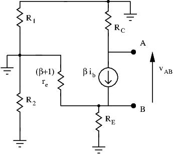
Let’s redraw our schematic with this small signal model of the BJT:
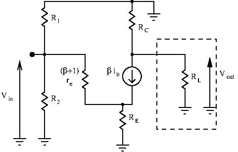
We can now find a relationship between  and
and  :
:
(3) 
![\[ v_{in} = V_B = R_E \times i_E + (\beta + 1) \times r_e \times i_B \]](http://modernhamguy.com/wp-content/ql-cache/quicklatex.com-2e925636f6e45ee1ff18481eda0fbc76_l3.png "Rendered by QuickLaTeX.com")
![\[ v_{in} \approx R_E \times i_C + \beta \times r_e \times i_B \]](http://modernhamguy.com/wp-content/ql-cache/quicklatex.com-3a762191c1f0913a3d4b0410cb188c96_l3.png "Rendered by QuickLaTeX.com")
![\[ v_{in} \approx R_E \times i_C + r_e \times i_C \]](http://modernhamguy.com/wp-content/ql-cache/quicklatex.com-e708559abd0200707babbb42cc29ab66_l3.png "Rendered by QuickLaTeX.com")
(4) 
We have expressions for and , and can now derive the voltage gain:
![\[ A_v = \frac{\Delta v_{out}}{\Delta v_{in}} = \frac{(R_C // R_L) \times i_c}{(R_E + r_e) \times i_c} \]](http://modernhamguy.com/wp-content/ql-cache/quicklatex.com-6ed99252395368c533254292a3d83021_l3.png "Rendered by QuickLaTeX.com")
(5) 
Adding the load changes the flow of current, and thus changes the real gain of the amplifier. For values  , the voltage gain becomes
  .
.
If we add the capacitor  , like is shown in most textbooks, disappears (capacitor is a short for AC, and the emitter resistance is bypassed) and the gain becomes:
![\[ A_v = \frac{R_C // R_L}{r_e} \]](http://modernhamguy.com/wp-content/ql-cache/quicklatex.com-ca4a423c3971e3507269425b07ad8d9c_l3.png "Rendered by QuickLaTeX.com")
Current Gain of the CE Amplifier
No calculation is necessary here. The ratio of output current  , and input base current
  , is simply the transistor’s current gain
  .
.
Input Resistance
Determining input and output resistance (or impedance) was always a mysterious art to me back in school. I never seemed to find the right answer. Worse still, years later when I’m once again trying to wrap my head around the concept, for the same simple circuit I get a different answer on every source I find. Some websites will even just say that the input resistance is “high”. Really? Wow, that’s helpful, thanks…
The reason you’ll find different answers on different sources is because they use different approximations and assumptions, which they often neglect to tell you about. In this section I’ll show you have to derive the input resistance of the CE amplifier
But first, what is input resistance? Input resistance is the the resistance seen by your input signal when going through your circuit.
Why do we need to know this value? Input and output resistance are fundamental concepts in the field of electronics, and even more so in RF engineering.
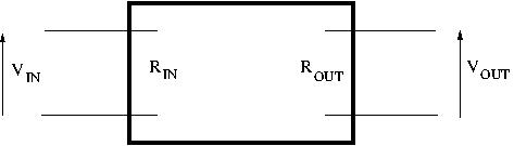
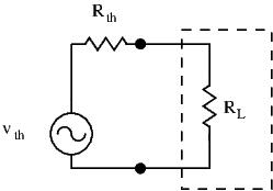
Take a look at the above diagram. Our amplifier, or any circuit really, can be simplified as a 2,3, or 4 port-network with a certain input resistance and a certain output resistance. Very often, we will use the 4-port network view. Any signal flowing through a circuit will face a certain resistance characteristic of that circuit. This is the circuit’s input resistance.
How does input resistance affect circuit behavior? Think back to Ohm’s law:  . If we increase
  , we decrease
  , and vice-versa. A high input resistance means the circuit will draw less current from the previous stage. The higher the input resistance of a circuit is, the less impact it has on the preceding circuit. The reverse is also true. A low input resistance will draw more current from the previous stage. The lower the input resistance of a circuit is, the more impact it will have on the preceding circuit.
There is a time and place for both high and low input resistance. One is not better than the other, it all depends on the circuit behavior we want to create. We will cover this in later chapters. For now, let’s calculate our amplifier’s input resistance.
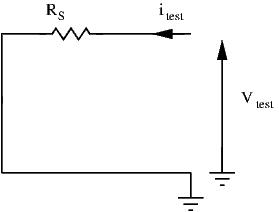
The academic way of finding a circuits input resistance is to apply a test voltage  at the input, and calculate the ratio
  . This is done on the small signal model of the circuit.
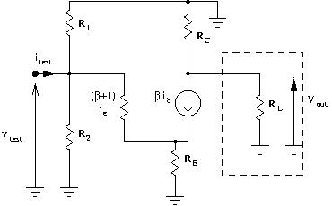
![\[ i_{in} = \frac{v_{in}}{R_1//R2//(\beta + 1) \times r_e} \approx \frac{v_in}{R_1//R_2// \beta \times r_e} \]](http://modernhamguy.com/wp-content/ql-cache/quicklatex.com-08653bd5e99c800070fc699ee1ba2776_l3.png "Rendered by QuickLaTeX.com")
Which gives us :
(6) 
In general, this is considered to be high, commonly in the thousands of ohms.
Output Resistance
Just as input resistance was resistance seen by a a signal entering the circuit’s input, output resistance is the resistance seen when looking into the output port of our circuit. Let’s use a simple example first to illustrate the concept:
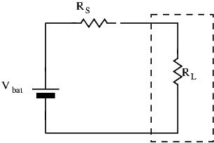
Take a battery for instance: all batteries have an internal resistance  . To the find the output resistance:
- Kill all independent powers sources (short voltage sources, open circuit all current sources)
- Remove the load
- Apply a test signal
 at the output terminal
 - Find the relationship:

For our battery, its very simple:
Using Ohm’s law, we immediately get  .
.
What does this tell us about the circuit? Output resistance is how vulnerable the circuit is with regards to its load. With a low output resistance, a lot of current can be drawn from the circuit’s output without changing the output voltage too much. On the other hand, a high output resistance will cause a circuit’s output voltage to drop quickly when current is drawn.
Having said that, let’s find the output resistance for our CE amplifier.
After removing the load, I’m left with:
But wait, what do I do with the current source present in my transistor model? It’s not an independent source, it’s value depends on our base voltage/current. It is a dependent source, and the above method for finding output resistance won’t work. So what do we do? We determine the equivalent Thevenin circuit of our amplifier. Remember, any circuit composed of a composed of a mix of resistances, voltage sources, and current sources, can be reduced to a single voltage source in series with a single resistor. Our small signal equivalent circuit fits this description, and we can thus use the Thevenin Theorem. Our goal is to obtain the following equivalent circuit:
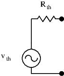
With circuits containing both independent () and dependent sources, the following steps can give us the Thevenin Equivalent circuit:
- Remove the load
- Find the open circuit voltage between nodes A and B. This voltage is the Thevenin equivalent voltage

- Short A and B, and determine

- The Thevenin Resistance is

You can choose any nodes to be A and B. Choose the one that makes the most sense.
Let’s follow these steps for our CE amplifier:
- Removing the load
- We choose our nodes A and B to be the output node and ground. Using these two nodes, no further simplification is necessary. Also, not really sure what other options there are here.
The output open circuit voltage is, using Ohm’s law:
![\[ v_{AB} = R_C \times i_c = R_C \times (\beta + 1) \times i_b \]](http://modernhamguy.com/wp-content/ql-cache/quicklatex.com-39c150cea7f1f6915cabccaaee609bd1_l3.png "Rendered by QuickLaTeX.com")
- Next, we short A and to determine

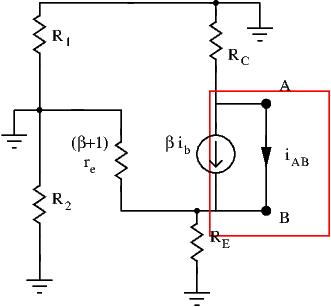 Look closely at the highlighted loop. is bypassed thanks to the short. The current flowing through AB is simply the current delivered by our current source. This gives us:
![\[ i_{AB} = (\beta + 1) \times i_B \]](http://modernhamguy.com/wp-content/ql-cache/quicklatex.com-6c12b6fd660431490524f63b116b5fc0_l3.png "Rendered by QuickLaTeX.com")
- We now know are our Thevenin Resistance:

Our output resistance is quite trivially our Thevenin Resistance, and is equal to , which is the value you’ll find in nearly all textbooks.
But what does this mean? Is high, low, or somewhere in between? To get an idea of the magnitude of you’ll find in most circuits, remember that our voltage gain was  . So, the higher we make , the higher our gain will be. In general, this means will be relatively high. So for our CE amplifier, the output resistance is moderately high.
That’s not great though. As we’ve learned in this section, high output resistance means our circuit is highly dependent on our load. We can amplify a signal with reasonable gain, but we can’t provide much current without our output voltage (and thus our gain as well) dropping rapidly. A solution to this problem will be shown in the following chapters.
Conclusion
Let’s go over all the characteristics of the CE amplifier that we’ve derived:


 : Moderately High
If you’ve made it this far, then congratulations! The tools you’ve learned in this chapter will serve you well until the rest of your electronics career or hobby. This is not an easy chapter to digest. If you’re relatively new to electronics, you might want to review this chapter over a few times to make sure you understand it. Also check out our beginner electronics series if you’re feeling a bit sketchy on the basics.
With these tools under your belt, you now have a reasonably good electronics culture. Let’s delve deeper!