Introduction
Why introduce a new device so soon? We haven’t even learned how to exploit BJTs yet, and already you’re being given even more weird devices! While it is true that most textbooks and course will have you study the BJT in more detail before introducing other semiconductors (and that’s how I first leaned too), I find that it makes the student too comfortable with just one kind of device, and they become afraid of using the others. Starting out with BJTs, studying them and using them, you will become increasingly comfortable with them. This is good, but the downside is you risk becoming afraid of committing the same amount of time and energy mastering other devices like the JFET. In truth however, if you can exploit a BJT, using Junction Field Effect Transistors, or JFETs, isn’t that different, as we will see.
How they are Made
JFETs come in two flavours: N-channel JFETs, and P-channel JFETs. Here are their corresponding electronic symbols:

Just like a BJT, a JFET has three ports: a gate, a drain, and a source. Electrons flow from the source and are collected by the drain. Gate voltage determines how much current is flowing from source to drain.
To understand how JFETs work, let’s take a deeper look at the N-channel JFET.
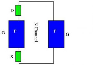
Just like BJTs, JFETs are made up of three layers of doped silicon. Unlike BJTs however, they are arranged differently. Whereas electrons had to transit through 3 different doped silicon layers in a BJT, in a JFET, electrons can flow from source to drain without crossing any PN junctions. For instance, in the N-channel JFET above, electrons can flow from source to drain via a single layer of N-doped silicon.
How they Work
If there is no PN juntion to cross, how do we control the current flowing through this N-channel? Notice how the N-channel is sandwiched in between the gate’s P-channel. What happens if we apply a negative voltage on the gate relative to the source (this is called reverse biasing the Gate-Source junction)? Remember that a PN junction acts like a diode and only allows current to flow in one direction. If we reverse bias the GS junction, we put the P-type silicon at a negative potential relative to the N-type silicon: no current can flow. However, this reverse biasing has consequences on the PN-junction. Let’s take a closer look at this junction.
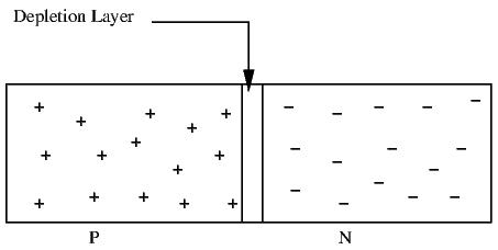
When no outside voltage is applied, a PN junction is in a state of equilibrium. Free electrons are present in the N-type silicon, and holes are present in the P-type silicon. At the junction however, free electrons can easily cross over to the P-type silicon to combine with holes. This creates negatively charged ions at the P-type silicon side of the PN-junction, and positively charged ions the N-type silicon side of the PN-junction. This creates an area with no free electrons or holes near the PN-junction. This area is called the depletion region and prevents conduction between the two regions. With no free electrons or holes, no more electrons can pass through the depletion region unless we forward bias the PN-junction.
By reverse biasing the PN-junction, we pull the holes from the P-type silicon away from the PN-junction. Likewise, we pull the free electrons of the N-type silicon away from the PN-junction. We are in effect widening the depletion region.

What does this mean for our N-channel JFET? Take a look:
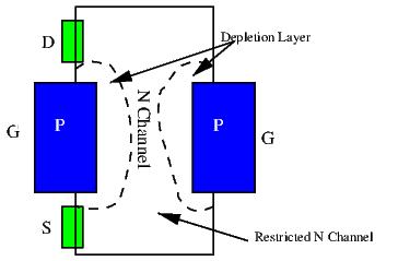
By widening the depletion region, we are restricting the area of the N-type silicon channel where electrons can pass freely, thus reducing the current. We are ‘pinching off’ the N-channel.
In an N-channel JFET, the more negative we make the gate, the less current will flow through the transistor.
Here lies one of the greatest differences between BJTs and JFETs: when no input signal is applied at the base, a transistor does not conduct. When no input signal is applied at the gate, the JFET conducts fully.
JFET Characteristics
We’ve seen how negative voltage at the gate relative to the source reduces current flow through the transistor. The point at which no more current flows is called the pinch-off voltage, or  .
.
By looking at the JFET’s characteristic curves found on any datasheet, we can easily spot this pinch-off voltage: look at the second curve below, and notice the point where  . The pinch off voltage here is around 6V.

Notice that there are two regions where the JFET can operate: the ohmic region, and the saturation region.
In the ohmic region,  increases almost linearly with
  . In this region, the JFET is simply a voltage controlled resistance.
In the saturation region, drain current is nearly independent of any change in gate to source voltage  . This is the region where we will do most of our work.
For any active device, we want to know the relationship between input and output. Here, input is the gate to source voltage , and output is the drain current . The following equation holds true in the saturation region only:
![\[ I_d = I_d_s_s*(1 - V_g_s/V_g_s(off))^2 \]](http://modernhamguy.com/wp-content/ql-cache/quicklatex.com-902cd4ceed4956fa8b1c564181f124f0_l3.png "Rendered by QuickLaTeX.com")
The JFET’s transconductance is defined as being:
![\[ g_m = \Delta I_d / \Delta V_g_s \]](http://modernhamguy.com/wp-content/ql-cache/quicklatex.com-d24ead7d620455473ce2d85c75970942_l3.png "Rendered by QuickLaTeX.com")
To be able to solve circuits that involve JFETs, we need to have an equivalent circuit to work with. Thankfully, the equivalent circuit of the JFET is quite simple:

Conclusion
From this chapter you need to remember five things:
- JFETs work opposite the way BJTs do: no voltage at the gate means maximum current flow. A JFET is a normally-on device.
- JFETs have two regions of operation: ohmic and saturation
- in the saturation region:


- the equivalent circuit of a JFET
Note that there are other types of transistors out there. However, for ham use, BJTs and JFETs cover the vast majority of all our use cases. We will cover other types of transistors much later in the course. For now, your basic working knowlegde of BJTs and JFETs is enough to start learning about transistor amplifiers.