![]()
I’ve noticed that very often, the first active device that students see if they study any kind of electronics past high school is the Op Amp, and only later are they introduced to the humble transistor. From a teaching point of view, I can understand this choice. Op Amps can be treated as a very simple black box, and feedback is incredibly easy to exploit and get across.
From a ham’s perspective however, transistors will come up in our designs very often, and learning to analyze circuits that use them is a prerequisite. Almost every ham circuit uses at least one of them. So let’s get started with the BJT – the Bipolar Junction Transistor.
How they Are Made
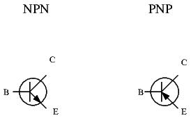
There are the two kinds of BJTs, the NPN transistor, and the PNP transistor. Here are their corresponding symbols:
They are named this way because of the way the different kinds of silicon layers are sandwiched together. Semiconductors are created by layering two different kinds of silicon in varying ways. These two different kinds of silicon are the N-type silicon and the P-type silicon.
N-type silicon possesses a lot of free electrons that, under the right circumstances, may move move to different atoms. To achieve this particular property, N-type silicon is doped (enriched) with an element that is able to give away its electron, a donor element. For those more chemically inclined, this doping element has 5 valence electrons, and is part of group 5A of the periodic table. Commonly used elements for N-type doping are Phosphorus and Arsenic.
P-type silicon, on the other hand, possesses a lot of holes. Holes are areas where electrons can easily go into: holes accept electrons. Chemically speaking, they correspond to an ’empty’ spot on the valence shell of P-type doping elements where electrons can come and go. So while N-type silicon can yield electrons, P-type silicon can receive electrons. P-type doping elements are part of group 3A of the periodic table, and possess 3 valence electrons. A commonly used element for P-type doping is Boron.
Note that, while doped silicon can yield or receive electrons, they themselves are electrically neutral and have no charge. They are simply enriched with neutral elements that happen to be able to yield or receive electrons, a useful property if we want to make electric circuits!
We’ve only scratched the surface of semiconductor manufacturing and properties. If all this seems a bit overwhelming to you, don’t worry, this was just to give you a bit of technological background on the devices we will use throughout our ham career. The main takeaway here is that semiconductors are made by sandwiching P-type and N-type silicon in different ways. Next we’ll see how these semiconductors actually work.
How it Works
Now we get to the interesting part! How does sandwiching P-type and N-type silicon actually accomplish anything? To explain this, let’s look at the NPN transistor in more detail.
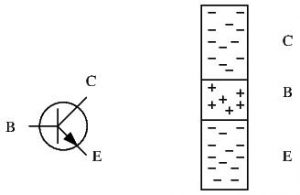
[insert vector graphics of NPN electrical symbol and NPN representation]
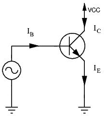
BJTs have 3 ports: base, collector, and emitter. Most circuits won’t have the ports labelled, so you’ll have to memorize the position of each port on the transistor. The base is easy enough to recognize, but many beginners (and more experienced hams and engineers as well) have trouble identifying which port is the collector and which is the emitter. If this is your case, just remember that the port which has the arrow will always be the emitter, whether it be an NPN or a PNP transistor. If you have trouble remembering which symbol relates to the NPN transistor, and which relates to the PNP transistor, you can use a simple mnemonic trick to remind yourself of the correct answer. NPN transistors have arrows that are ‘Not Pointing iN”.
In an NPN transistor, as the diagram shows, both the collector and emitter are made of N-type silicon: the emitter and the collector are able to yield electrons. Let’s connect the collector to a positive voltage source and ground the emitter, as shown:
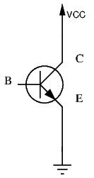
What happens then? Well, nothing at all! Our goal is to allow current to flow from the positive voltage source to ground, which means allowing electrons to flow from ground to the positive voltage source. In fact, in a BJT, the role of the emitter is to send electrons, and the role of the collector is to receive these electrons. This way, current flows from the collector to the emitter. Due to the nature of the doped silicon, electrons can easily travel from electron-rich N-type silicon to the electron-poor P-type silicon. However, it is very difficult for electrons in the P-type silicon to travel to the N-type silicon. In the above diagram, simply connecting the collector to a positive voltage source and grounding the emitter isn’t enough to make current flow through the transistor.
To overcome this barrier, we can apply a positive voltage source to the base of the transistor.
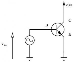
This will force current into the base and out the emitter, or force electrons through the emitter and into the base. For a simplified explanation: the positive charge of the base will attract electrons from the emitter up to the base, and once there, the positive charge of the power supply connected to the collector will attract the electrons from the base through the collector. For this to work, a small amount of electrons is ‘wasted’ and sunk into the base. The more electrons are sunk into the base, the more electrons also pass through the transistor from ground to the power supply. Said otherwise, the more current we inject in to the base, the more current will flow through the transistor.
While the above paragraph isn’t technically correct, it is a good place to start to understand how a BJT works. More detailed analysis of the inner workings of transistors are widely available on the web and in classic textbooks. For our needs however, an intuitive feel of the physics behind semiconductors is enough to get us going.
Notice we can change the behavior of the transistor by modifying the base current. We can make the transistor allow a lot of current to pass, only a small amount of current to pass, or to stop conducting all-together. This is way transistors belong to the semiconductor family.
Characteristics of BJTs
We just saw that BJTs are composed of three layers of doped silicon. Both NPN and PNP transistors then contain 2 PN junctions. A PN junction is the area where the P-type silicon and N-type silicon meet. As said in the previous section, it is easy for electrons to travel from the N-type region to the P-type region, but the reverse requires much more energy. A PN junction is simply a diode, allowing current to flow in only one direction (from P to N). A diode is also a semiconductor.
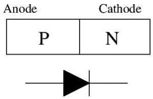
This is useful to know because a part of our transistor acts like a diode. Specifically, for an NPN transistor, the base-emitter junction functions as a diode. For a PNP transistor, the emitter-base junction functions as a diode. This is easy to remember, just locate the arrow on each transistor symbol: it will show you the ‘diode’ part of the transistor.
We know that when diodes conduct, there is a voltage drop across the diode equal to around 0.7V (or 0.2V for a germanium diode). We then have our first transistor characteristic. For an NPN transistor:
![\[ V_b_e = V_b - V_e = 0.7 V \]](http://modernhamguy.com/wp-content/ql-cache/quicklatex.com-f10b038c8df6978a1f26bc909312893b_l3.png "Rendered by QuickLaTeX.com")
We also mustn’t let  : the base-emitter junction must always be forward biased (more positive at the base than at the emitter)
For a PNP transistor!
![\[ V_e_b = V_e - V_b = 0.7 V \]](http://modernhamguy.com/wp-content/ql-cache/quicklatex.com-5775c2834ed71660a26833b6f5eede3d_l3.png "Rendered by QuickLaTeX.com")
We mustn’t let  : the emitter-base junction must always be forward biased.
We still haven’t explained how transistors can amplify signals. As said previously, a control signal flowing into the base can command a much greater flow of current to flow through the collector and emitter. That flow is orders of magnitude higher than the control signal. We have amplification. A transistors current amplification ratio is written as  , or beta:
![\[ i_c = \beta \times i_b \]](http://modernhamguy.com/wp-content/ql-cache/quicklatex.com-039dc413c9cc76df14c2166dda0a3b87_l3.png "Rendered by QuickLaTeX.com")
That amplification is not free of course, the transistor needs to be connected to a power supply to be able to deliver the wanted current (the collector is connected to  ).
).
Often, it may be easier to work with input voltage instead of input current. is a transistor’s current gain, connecting base current to collector current, and has no unit. Another popular quantity that is important to understand is the relationship linking control voltage and output current. We call this a device’s transconductance  .
.
![\[ i_c = g_m \times v_b_e \]](http://modernhamguy.com/wp-content/ql-cache/quicklatex.com-9ee874695f15341cca038278f301916f_l3.png "Rendered by QuickLaTeX.com")
BJT Equivalent Circuit
It is difficult to analyse a circuit containing transistors outright. To simplify the process, we need to use a representative model of our transistor so we can then apply our tried and true electronic circuit theory methods to solve it.
Depending on the frequencies our circuit will need to handle, we will choose different models. To start our education in the realm of transistors, let’s take in the simplest of these models, valid for low frequency applications:

Between collector and emitter we have a dependent current source, giving a current of  . Straightforward enough. But what is
  in the base to emitter resistance? Is it linked to one of the characteristics we discussed earlier?
Let’s consider the emitter grounded. We then have:
![\[ V_b_e = V_b = V_i_n \]](http://modernhamguy.com/wp-content/ql-cache/quicklatex.com-7975db1fff019b0b4d822c5825f18042_l3.png "Rendered by QuickLaTeX.com")
Thus, we have:
![\[ I_i_n = I_b = \frac{V_{in}}{(\beta+1)r_e} \approx \frac{V_{in}}{\beta \times r_e} \]](http://modernhamguy.com/wp-content/ql-cache/quicklatex.com-8769b6333126047d8c87d89db3bcdd63_l3.png "Rendered by QuickLaTeX.com")
With these equations, we can find the relationship between beta and :
![\[ I_b = \frac{V_{in}}{\beta \times r_e} \]](http://modernhamguy.com/wp-content/ql-cache/quicklatex.com-08839597ea2ca1065e5f7c1a942aeca2_l3.png "Rendered by QuickLaTeX.com")
![\[ V_{in} = \beta \times r_e \times i_b \]](http://modernhamguy.com/wp-content/ql-cache/quicklatex.com-49d378ed37236f9f1c43f9a60e44af04_l3.png "Rendered by QuickLaTeX.com")
Since  , we have
![\[ I_c = \frac{V_{in}}{r_e} \]](http://modernhamguy.com/wp-content/ql-cache/quicklatex.com-66427f87c0d607b63bb45c391f7a5d4a_l3.png "Rendered by QuickLaTeX.com")
Since  , we have
![\[ g_m = \frac{1}{r_e} \]](http://modernhamguy.com/wp-content/ql-cache/quicklatex.com-b1d7ae33da29145754d94e44bfd271a7_l3.png "Rendered by QuickLaTeX.com")
is the inverse of our transistor’s transconductance (in Siemens) . is indeed a resistance, expressed in Ohms.
can be explained as being the resistance seen from the base to the emitter. Think of it as an internal resistance the emitter has. Its value changes based on the emitter current, and is equal to:
![\[ r_E = \frac{26}{I_E} \]](http://modernhamguy.com/wp-content/ql-cache/quicklatex.com-5ca67531326a44e672c7401e17dcbdb0_l3.png "Rendered by QuickLaTeX.com")
With  in Ohms, and
  in mA. This value will prove to be quite useful to us for our calculations later on.
Conclusion
So far, we have covered how a transistor works, as well as 3 essential things to remember:
- a transistor has a current gain of :

- a transistor’s transconductance is

- the low frequency equivalent circuit of a BJT