Introduction
When I first learned all my classical amplifier circuits, I naively imagined I’d be able to understand any amplifier circuit I came across. Oh how wrong I was. I thought I’d find the exact same configurations I worked through when studying transistor amplifiers in real life circuits too. I quickly found out that just knowing your classical amplifier configurations is not enough.
Just because you’ll rarely find the classical amplifier circuits copy pasted into real life designs doesn’t mean all that hard work and study was for nothing however! No matter what kind of added circuitry you find, a transistor will always be used in one of the three configurations we previously studied (Common Collector, Common Emitter, Common Base, or, for JFETs, Common Drain, Common Source, and Common Gate). By identifying the input and the output, you’ve already understood quite a lot about the amplifier. You already what configuration it is in. Even if the amplifier doesn’t look exactly like what you know, you’ll already have a good idea of its general properties (voltage gain, current gain, input resistance, output resistance).
But, as future circuit designers, we want more than a general idea of what a circuit does. We want to know exactly why that extra part was added, and how it affects circuit behavior.
This chapter will try and categorize as many common “tricks” as possible circuit designers use for their amplifiers to fit their design cases. This is definitely not an exhaustive guide, but hopefully the examples given here will help you make more sense of the majority of RF amplifiers out there in the ham literature.
The Most Common Amplifier
You’ll notice all the examples in the following paragraphs will be variations on the Common Emitter amplifier. For reason for this is that the CE amplifier is by far the most common one you will find in the ham world. And, as said above, you’ll rarely find it as it was presented in your college textbook. However, a few variations of the CE amplifier come up very frequently, so it us useful to understand them. Let’s see what they are and why circuit designers use them.
Case#1 : The Decoupling Resistor
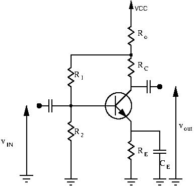
The difference between the above schematic and the classical Common Emitter amplifier is the  resistor. What does it do? Without doing any math, let’s try and gain an intuitive understanding of its function.
If the input voltage  increases, more current will flow through our transistor, and thus also through
  and . But, if more current flows through , knowing Ohm’s Law, a higher voltage drop will occur through . This will cause
  to decrease, thus decreasing the bias voltage and current ( being lower, so will
  ). The decreased bias voltage will make the transistor conduct less current, therefore lowering the gain.
To recap, if increases, the circuit will want to decrease . If decreases, the opposite happens and the circuit will want to increase .
The role of is to stabilize the bias. It adds negative feedback to our circuit. Don’t worry if you don’t get negative feedback yet, we have whole chapters dedicated to it later on in the course.
is called a decoupling resistor, and its value is relatively small compared to the other resistances in the circuit. The higher is, the higher the voltage drop across it will be, and the lower the driving bias voltage will be, therefore decreasing gain. Frequently, you will find to be in the range of the hundreds of ohms at most.
Case #2: Inductors at the Collector
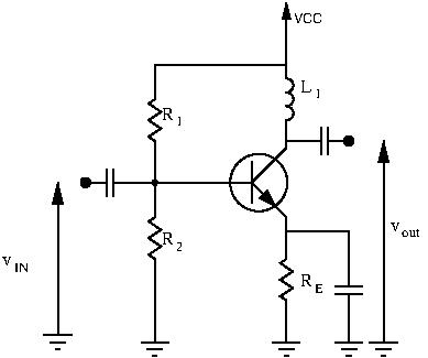
At first glance this circuit is useless. The DC gain for this circuit is nil (inductor is a short for AC signals). Why place an inductor there? The answer becomes clear when you look at large RF signals.
If we add a load, the AC gain for this circuit is  . The gain depends on emitter current biasing and on the load resistance. To understand the usefulness of the inductor, let’s recall the formula for the voltage drop across a resistor and the voltage drop across an inductor:
- for a resistor, using Ohm’s Law:

- for an inductor:

 can only go one way: it will always be a voltage drop. No matter what the input signal is, the current
  will always be positive. Thus, in a typical common emitter configuration, collector voltage will always be less than or equal to
  .
.
 , on the other hand, can go both ways. can be either positive or negative. If
  , then
  , and the collector voltage will become higher than .
How can this be useful? If we were only using resistors, our voltage excursion at our output will be limited to a maximum of  (remember, collector voltage must always be higher than base voltage).
But, if our collector voltage is no longer limited to thanks to the inductor, we can increase our voltage excursion at our output, and thus also increase our power output.
For maximum power delivery, we want maximum voltage excursion without distortion. If we are no longer bound by at the collector, then the most we can possibly get is  both ways. Why is that? With no signal applied, collector voltage will be , so the most the collector can go down is , since we can’t let collector voltage drop below base voltage. If the collector voltage can’t go down more than from its quiescent value of , then the most is can swing upwards is also . Thus the maximum possible voltage spread is twice .
For maximum power delivery, ideally we want current excursion to also be maximized: collector current should range from near zero to twice the bias value.
To get both maximum voltage and current excursions, we need to choose a specific load  , given to us by Ohm’s law:
![\[ R_L = \frac{\Delta V}{\Delta I} = \frac{2 (V_{CC} - V_B)}{2 I_E} = \frac{(V_{CC} - V_B)}{I_E} \]](http://modernhamguy.com/wp-content/ql-cache/quicklatex.com-01628da73f3c80f9df927a4485659d15_l3.png "Rendered by QuickLaTeX.com")
What happens if is not equal to that value? Then a mismatch occurs between current and voltage excursions:
- if is too low: the transistor will be current limited: too much current is asked of the circuit. High current excursion, but low voltage excursion
- if is too high: the transistor will be voltage limited. High voltage excursion, low current excursion
When should you use an RF choke at the collector? It is not very useful for small signal operations, but rather more often used for power applications (large signal applications).
Case #3: Negative Feedback
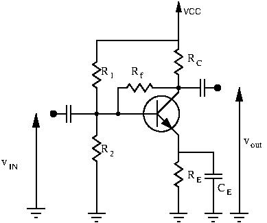
Whenever you see a portion of the output fed back into the input of the circuit, you have feedback. When that feedback acts as to reduce overall gain, you have negative feedback.
Intuitively, without doing any math, we can already see the purpose of  . As
. As  increases, collector current increases, causing collector voltage
  to decrease. This causes less current to flow through , and thus causes the base voltage
  to decrease. This causes collector current to decrease, decreasing overall gain.
Negative feedback decreases gain, but that’s not all it does. Feedback is a very powerful tool for circuit designers, and many chapters will be dedicated to it in the near future. For now though, just keep in mind that negative feedback increases amplifier bandwidth and stability at the cost of gain.
Case #4: Transformer Coupled Collector
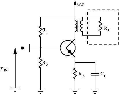
Recall case #2. With the collector voltage no longer bound by , we were able to deliver more power by carefully choosing our load. However, in real life scenarios our load is already chosen for us. In this case we have to transform this output load into something the collector wants to see. There are 2 ways to do this: impedance matching networks, or RF transformers.
Conclusion
These 4 cases cover a lot of the variations you will see of the common emitter amplifier. Hopefully the above examples will stop you from scratching your head too much when looking at radio circuits. For negative feedback, there are many more variations possible, and the math behind it is quite gruesome. Negative feedback will be explained, with all the mathematical details, in another chapter.