Introduction
The last of the JFET classical amplifier configuration is the common gate amplifier, analogous to the common base BJT amplifier. As usual, we will derive the voltage gain, current gain, input resistance, and output resistance of this configuration.
The Common Gate Amplifier
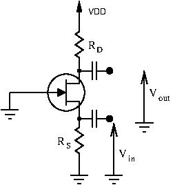
For the common gate amplifier, the input signal is applied at the source, while the output signal is sampled at the drain. As you can see, the gate itself is grounded: the gate is “common”.
Voltage Gain
To derive the voltage gain, let’s draw the small signal equivalent circuit:
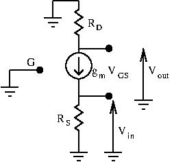
As usual, let’s express  and
and  to find the voltage gain
  :
:

 , with
  because the gate is grounded
Substituting  in the first equation gives:
![\[ v_{out} = V_{CC} + R_D g_m v_{in} \]](http://modernhamguy.com/wp-content/ql-cache/quicklatex.com-e428101e77bf91a6e54c974bdda927eb_l3.png "Rendered by QuickLaTeX.com")
We can now calculate our voltage gain:
![\[ A_v = \frac{\Delta v_{out}}{\Delta v_{in}} = R_D g_m \]](http://modernhamguy.com/wp-content/ql-cache/quicklatex.com-dc1ca68547b49a6756f29fc39ea46e90_l3.png "Rendered by QuickLaTeX.com")
If we add a load, this gain becomes 
Current Gain
To find the current gain, we need to add a load, and determine the input and output current.
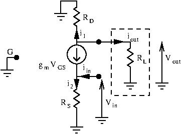
Let’s express  . A node equation at the source terminal gives us:
![\[ i_{in} = g_m v_{GS} - \frac{v_{in}}{R_S} \]](http://modernhamguy.com/wp-content/ql-cache/quicklatex.com-ac72a9fd090867b9df3d07dcc78879eb_l3.png "Rendered by QuickLaTeX.com")
Since  (gate is grounded), we have:
![\[ i_{in} = -g_m v_{in} - \frac{v_{in}}{R_S} = -v_{in}(g_m + \frac{1}{R_S}) \]](http://modernhamguy.com/wp-content/ql-cache/quicklatex.com-80b5793a85ef871f5bbedca264200319_l3.png "Rendered by QuickLaTeX.com")
Let’s express  next, using ohm’s law. We already know the output voltage since it was calculated in the previous section.
![\[ i_{out} = \frac{v_{out}}{R_L} = \frac{g_m R_D // R_L v_{in}}{R_L} \]](http://modernhamguy.com/wp-content/ql-cache/quicklatex.com-e7726fbc34c6eb804a0f3f67e6201945_l3.png "Rendered by QuickLaTeX.com")
We can now derive the current gain  :
:
![\[ A_i = \frac{i_{out}}{i_{in}} = \frac{g_m R_D // R_L}{R_L} \times \frac{1}{g_m + \frac{1}{R_S}} \]](http://modernhamguy.com/wp-content/ql-cache/quicklatex.com-fe9e627bc60c8b55e9161fb45db737c0_l3.png "Rendered by QuickLaTeX.com")
![\[ A_i = \frac{g_m R_D // R_L}{R_M} \times \frac{R_S}{g_m R_S +1} \]](http://modernhamguy.com/wp-content/ql-cache/quicklatex.com-76ba80156d848730577e2efeb42378f5_l3.png "Rendered by QuickLaTeX.com")
By approximating  , we obtain:
![\[ A_i = \frac{g_m R_D // R_L \ times R_S}{R_L g_m R_S} = \frac{R_D // R_L}{R_L} \]](http://modernhamguy.com/wp-content/ql-cache/quicklatex.com-91f92f5be6af783a2a159cec4e360f70_l3.png "Rendered by QuickLaTeX.com")
As we can see,  . Our current gain is less than unity. For
  relatively low compared to
  , we have
  . This is why you will often see people say the common gate amplifier has unity current gain.
Input Resistance
To find the input resistance, we apply a test signal at the input and calculate  :
:

 , node equation at the source terminal
This gives us:  .
.
The input resistance of the common gate amplifier is low.
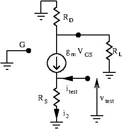
Output resistance
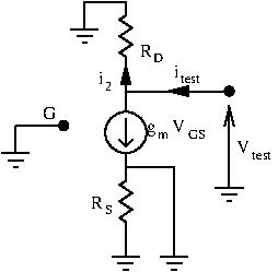
To find our output resistance, we remove the load and ground the input. Then, we apply a test signal at the output and calculate  .
.
Using a node current equation at the drain terminal, we have:
![\[ i_{test} = -\frac{v_{test}}{R_D} - g_m v_{GS} \]](http://modernhamguy.com/wp-content/ql-cache/quicklatex.com-e5855401e93de431842df3c7905f24cb_l3.png "Rendered by QuickLaTeX.com")
However, since the gate and source are grounded (source is grounded because we grounded the input), we have  . This gives us:
![\[ i_{test} = -\frac{v_{test}}{R_D} \]](http://modernhamguy.com/wp-content/ql-cache/quicklatex.com-13d411da5b5a5902915cb5c3fa90862e_l3.png "Rendered by QuickLaTeX.com")
And thus, our output resistance is . This is considered high.
Conclusion
To recap, the common gate amplifier has:
 , a high voltage gain
- , unity current gain
 , a low input resistance
 , a high output resistance
As expected, the common gate amplifier has very similar properties to the common base amplifier.