Introduction
We’ve learned about the basics of feedback circuits in the previous chapter. Now is the time to actually see how we can exploit feedback to our advantage. In this chapter we’re going to go through the necessary steps to exploit negative feedback in a transistor amplifier circuit. To make things more interesting and more useful, circuit simulation using QUCS (Quite Universal Circuit Simulator), an open-source circuit simulator with an easy to use GUI interface, will be used to verify our claims.
Circuit simulation is a blessing for circuit designers, if used properly. Basic electronic theory and rules of thumb are still necessary to rough out your design. Using simulation you can quickly test your theoretical circuit and see which values need tweaking. We’ll delve deeper into circuit simulation in future posts.
How we Exploit Negative Feedback
In the previous chapter, we learned that an amplifier with negative feedback had a gain of  ,
,  being the open loop gain (the gain the circuit would have without negative feedback). Using negative feedback, we can drastically reduce the effect of variability in gain of active devices, and thus more accurately control the gain, since with a high enough
  , the gain will depend mostly on the feedback network
  .
.
All feedback amplifiers work on the same principle: make a circuit with huge, poorly controlled gain, and then use a feedback circuit to greatly reduce the gain, but at same time make it much more stable.
A Transistor Amplifier Example
Too illustrate our point, let’s give an example, using our commonly known transistor amplifier circuits. Unfortunately, single transistor amplifiers don’t produce huge amounts of gain, and it’s difficult to get more than 100 out of one stage. A common way to get more gain out of transistor circuits is to cascade similar amplifiers. It is, of course, still possible to use negative feedback on single transistor amplifiers,
But, first, let’s design a simple Common Emitter amplifier.
One Transistor Amplifier
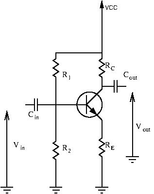
We will use the very common general purpose 2N3904 NPN transistor. Let’s fix our design constraints:

- Collector current
 : according to the datasheet, current gain
  is highest at this value
  , on the low end of the available range, giving us a conservative estimate
- Voltage gain

 (using half
  is usually a good choice and allows a good amount of output voltage swing)
We need two equations to determine  and
and  . A KVL loop from to ground gives us:
![\[ V_{CC} - R_C I_{CQ} - R_E I_{CQ} - V_{CEQ} = 0 \]](http://modernhamguy.com/wp-content/ql-cache/quicklatex.com-1741842473aef0722066a182b13778ad_l3.png "Rendered by QuickLaTeX.com")
Which gives:
![\[ R_C + R_E = \frac{V_{CC} - V_{CEQ}}{I_{CQ}} \]](http://modernhamguy.com/wp-content/ql-cache/quicklatex.com-339511b33308b58520fdaeb00dff6a51_l3.png "Rendered by QuickLaTeX.com")
Our voltage gain  gives us our second equation, and this we find:


To find the biasing resistors  and
and  , we first need to determine, approximately (remember, varies from transistor to transistor) the base current. Base current here is
  .
.
For proper biasing, a common rule of thumb is to make the current flowing through the bias resistors at least 10 times the bias current. The current flowing through and is thus 
We find the base voltage 
We can now find to get the proper bias current:
![\[ V_B = V_{R2} = R_2 \times I_{bias} \]](http://modernhamguy.com/wp-content/ql-cache/quicklatex.com-e807311565ccb5f5257cf8eec0a6de3b_l3.png "Rendered by QuickLaTeX.com")
Which gives us:
![\[ R_2 = \frac{V_B}{I_{bias}} = \frac{1.15}{670.10^{-6}} = 1716 Ohms \]](http://modernhamguy.com/wp-content/ql-cache/quicklatex.com-cd1bdde8838ab4da6f739f0f4544e1a4_l3.png "Rendered by QuickLaTeX.com")
Lastly, we need , which is easily found with Ohm’s Law. The voltage drop across is : 
This gives us: 
We have our final circuit, here drawn in QUCS:
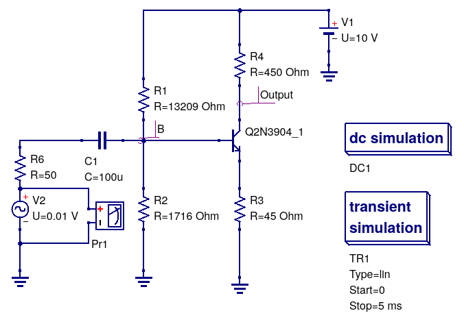
Don’t mind the impossible resistor values here, this example is not meant to be reproduced in real life, and serves just as a teaching example. Notice here that we’ve added a source resistance after our AC input voltage source, equal to  . The signal coming from our input follows a certain resistance. In RF design, very often our signal will come from a 50 Ohm transmission line, hence the 50 Ohm resistance. If the signal comes from a laboratory signal generator, very often it will have a 50 Ohm source resistance as well. This value can usually be found in the datasheet.
Notice also the AC-coupling capacitor value. It is huge, at  . The reason for this is the frequency I’ve chosen for the input signal: only 1 kHz. The lower the frequency, the higher the coupling capacitor value will have to be. To come up with this value I simply toyed around with a several values in the simulator and chose one that gave acceptable results (aka having the full swing of the input signal translated at the transistor base).
Don’t fret if you don’t understand what is it I’m doing with the software. I’ll have a small chapter dedicated to circuit simulation in the future. After simulation, we have the following graphs
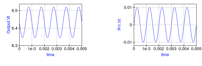
The gain is approximately 10, which is what we designed for.
Cascaded Amplifiers
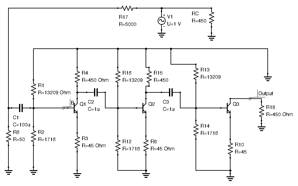
A voltage gain of 10 isn’t a lot. If we use feedback on this circuit, our gain will drop. We don’t have much gain to begin with, so before playing around with feedback, we need to increase the gain. We’ve already designed one Common Emitter amplifier. All we need to do now is cascade a few of them together to multiply the gain. Our goal is to use negative feedback, so we will use an odd number of stages. This way the last stage’s output voltage will be 180 degrees out of phase with the input. Feeding it back into the input will provide negative feedback. Using an even number of stages, the voltages will add, creating positive feedback and driving our circuit into saturation.
That said, stacking 3 of these amplifiers should give us an open-loop gain of approximately 1000:
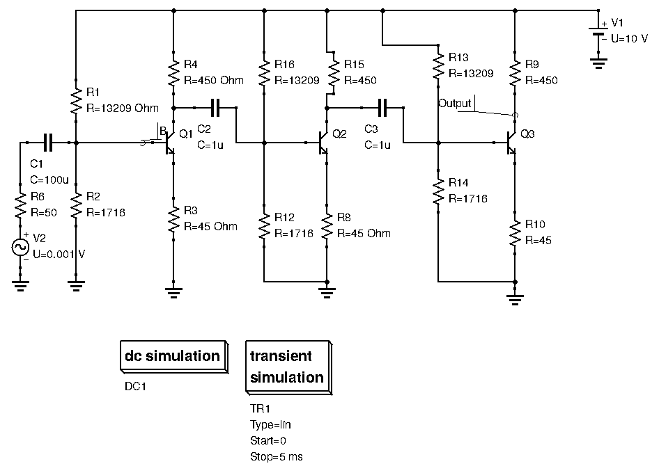
Launching the simulation however, our overall gain seems to be only around 400. This is due to improper impedance choice. Ideally, we want low output resistance and high input resistance. In our example however, the output resistance of our Common Emitter amplifier is  , while the input resistance is less than
  . hardly dominates , hence voltage divider effects are in action, reducing overall gain. We’ll talk more about properly cascading amplifiers in later posts. For now, a gain of 400 is good enough for our purposes.
Adding Feedback
Now, let’s add feedback:
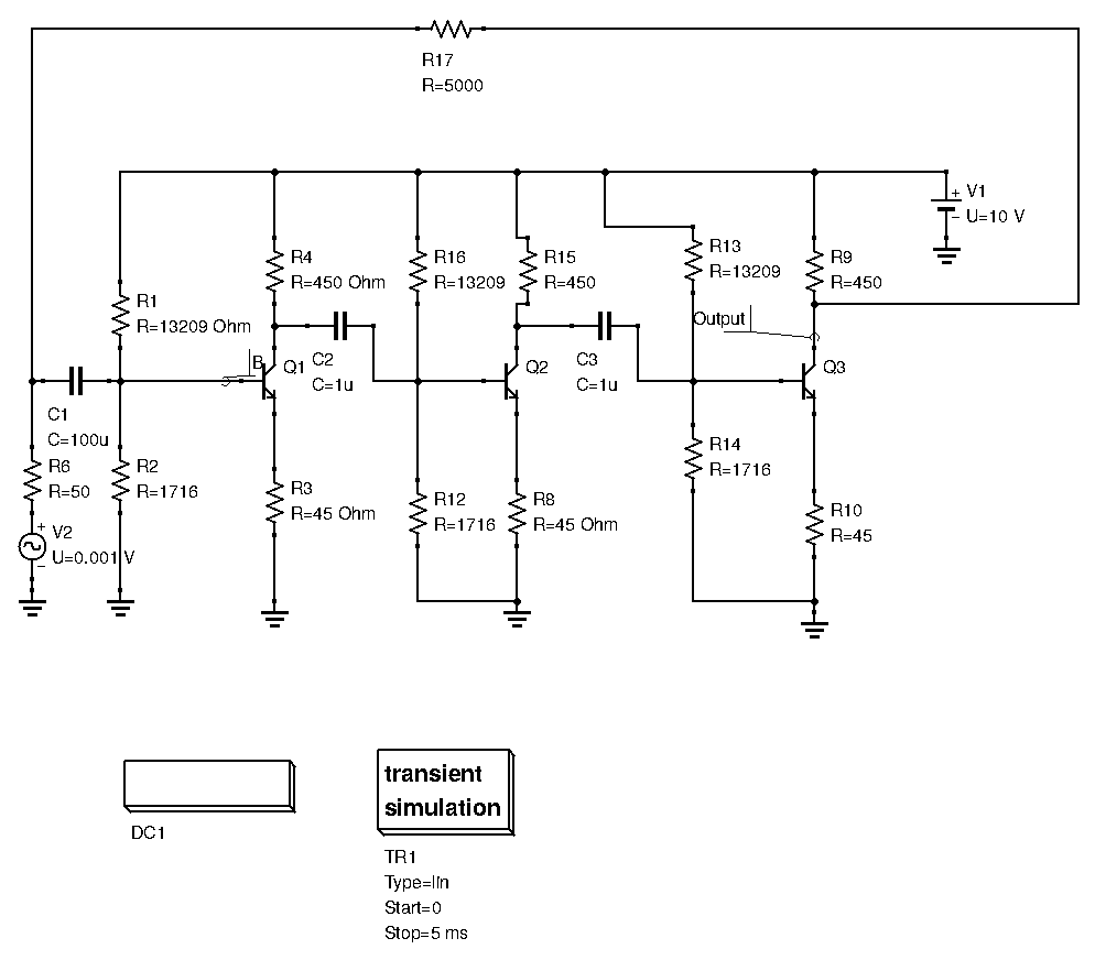
 is our feedback resistance
  .
.
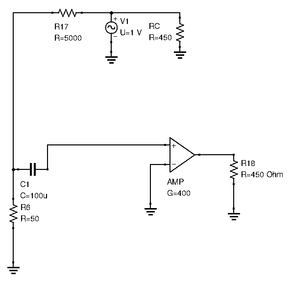
The higher is, the lower the amount of current that is fed back into the input. Hence, a higher means lower feedback, whilst a lower means a high feedback. This whole scheme is starting too look complicated, lets simplify the circuit:
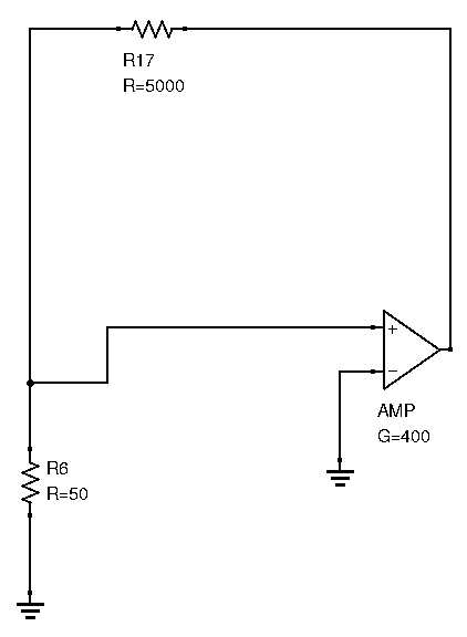
The whole 3 stage amplifier can be modeled as a block with gain  . The source resistance
  being so low compared to the other resistances, we can ignore all other input resistances. The feedback network then is solely dependent on the voltage divider resistor network formed by
  and . The feedback network divides the output voltage by
  , hence
  . By choosing
  (as an example, nothing more to it),
  , and the loop gain
  is then
  . We can then calculate the closed loop gain
  .
.
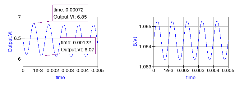
With feedback, our gain is reduced from 400 to 80. Let’s see if the simulation confirms this:
Our simulation gives us a gain of around 80 (to calculate the gain I simply divide the peak to peak voltage of the output with the peak to peak voltage of the input. Peak to peak voltage for our input is 0.002V).
Some Considerations
Now, the above feedback amplifier isn’t great. The different stages aren’t properly cascaded, and the loop gain is very low. To truly reap all the benefits of negative feedback, we ideally want a higher loop gain, at least 20. This way, the open-loop gain of the circuit becomes irrelevant.
Also, be aware that the values for resistances we used here are definitely not standard values. You can’t build this circuit! This was just to illustrate a concept. Of course, if you were to reproduce this circuit with real components, you would constrain all resistor values to the nearest standard value. The circuit’s behavior shouldn’t be grossly affected by the change.
The Problem with
In this example finding the feedback network was relatively easy. In fact, the block diagram we introduced in the previous post implies that the feedback network is easy to find and independent of any other circuitry.

Unfortunately this is not always the case. Often times the feedback network is intertwined with biasing components and the active device itself, making identifying nearly impossible. In such cases, there is a universal method that allow us to determine the loop gain, without having to find .
Determining the Loop Gain
The universal method of determining loop gain in a negative feedback amplifier has 5 steps. Once you’ve identified the feedback loop:
- Kill voltage and current sources. That is, ground all voltage sources, and open circuit all current sources.
- Cut the feedback loop at any point.
- Before the cut, insert the equivalent resistance that the circuit saw before cutting the loop.
- After the cut, insert a test signal: either a voltage source or a current source.
- Make the test signal travel the loop, and calculate the ratio of the two currents (or voltages if a voltage source was chosen)
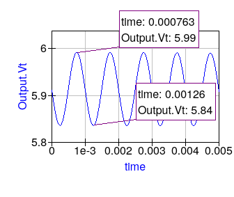
Lets use the previous 3 stage amplifier an example:
- We kill all the voltage and current sources
- As shown above, we cut the loop at the collector of the last transistor stage.
- We add a resistance equal to the value the collector saw at its output. The collector resistance being very small compared to the feedback resistance, we just replace it with .
- A test voltage signal was applied after the cut.
- The three stage amplifier circuit can be modeled as a simple block with a voltage gain of 400: as follows:
 Thus, base voltage becomes
  , and output voltage becomes
Our voltage ratio is: Numerically, this evaluates to 4. Our loop gain is 4, the same result as found above.
Conclusion
Feedback can be a difficult subject to wrap your head around. Many people are able to easily exploit Op-Amp feedback circuits, but get stuck when studying even simple transistor circuits with feedback. Just remember that to exploit negative feedback in any circuit, you need to:
- Make a circuit with huge gain, however inaccurate or unstable it may be.
- Add negative feedback to drastically reduce the gain, whilst also greatly increasing predictability reproduce-ability.