The Phase-Locked Loop (PLL) is one the most popular building blocks of any RF system. Understanding the PLL unlocks many possibilities for the experimenter, however many hobbyists and those relatively new to electronics are put off by its apparent complexity. While PLLs can seem daunting, by understanding the main principle behind PLL theory and dissecting each functional block of a PLL system, we can hopefully familiarize ourselves with this fascinating technology and apply it to our own designs.
How do Phase-Locked Loops Work?
Before getting into the actual architecture of a PLL, it’s best to first explain what fundamental concept is used in a PLL. That concept is phase comparison. If you take two signals and compare their phases over time, two cases are possible:
- The phase difference changes: the frequencies of the two signals are different
- The phase difference stays the same: the frequency of both signals is equal
To better visualize this phenomenon, let’s create two different signals, and represent them on a phase diagram, from 0 to 360°:
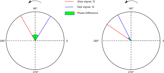
In this representation, signals turns at a speed equal to their frequency. The angle difference between both signals is the phase difference. Hence, a signal with a higher frequency will spin faster. Therefore, if we compare two signals with different frequencies, they will “spin” at different speeds. When comparing their phases, the phase difference will constantly change. On the contrary, two signals with the same frequency will spin at the same speed: the phase difference will stay the same.
PLLs function on the premise that two signals with the same frequency will have a constant phase difference.
PLL Building Blocks
Now that we understand phase comparison, let’s look at the actual architecture of a Phase-Locked Loop:
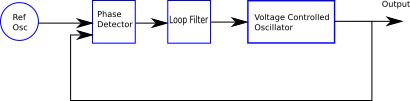
If you’ve studied feedback, or have seen my posts on it, you’ve probably noticed that this looks a lot like a feedback loop., and you’d be right. The PLL is a system that relies on feedback to work. Let’s dive deeper into the PPL’s architecture and study each block in more detail:
Reference Frequency
The reference frequency can be thought of as the PLL’s master frequency, against which the output of the PLL will be compared. This reference frequency needs to be accurate and stable. Indeed, the performance of the final PLL system depends heavily on this reference oscillator. Very often, a fixed crystal oscillator is used for this purpose.
Phase Detector – Type I
PLL’s are often confusing to beginners because how they blend digital and analog electronics. Not all PLLs look the same, and their building blocks, even if they have the same name, and ordered the same way, can have vastly different internal circuitry. Such is the case for the phase detector. There are two possible types of phase detectors, and depending on whether we want to work with analog or digital signals, we may choose one over the other.
The first type of phase detector is the type I phase detector. This detector can work with either digital or analog signals. To understand how an analog version of this phase detector could be built, let’s do some math first. Our goal is to find the phase difference of two different signals:
![\[ s_1 = \sin(\omega_1 t) = \sin(\alpha) \]](http://modernhamguy.com/wp-content/ql-cache/quicklatex.com-fed4416be4bb07e800d2349fd2f26225_l3.png "Rendered by QuickLaTeX.com")
![\[ s_2 = \sin(\omega_2 t) = \sin(\beta) \]](http://modernhamguy.com/wp-content/ql-cache/quicklatex.com-aa3adebbefd234ff85a4d69ca3770d89_l3.png "Rendered by QuickLaTeX.com")
Finding the phase difference of these two signals would mean extracting the phase of both signals with an  function somehow. In analog circuitry, this would be extremely complex and probably unreliable. Instead, we can cheat and exploit a trigonometric approximation to ease the job. For small values of a we have:
![\[ \sin(a) \approx a \]](http://modernhamguy.com/wp-content/ql-cache/quicklatex.com-e2edc79e6497bcd9433b22c74726326f_l3.png "Rendered by QuickLaTeX.com")
There fore, as long as  is small enough, we have:
![\[ \sin(a-b) \approx a-b \]](http://modernhamguy.com/wp-content/ql-cache/quicklatex.com-422f8b1ca913f55244fe31ae5b080706_l3.png "Rendered by QuickLaTeX.com")
Great! So the  of our phase difference can be approximated as the phase difference itself. This greatly simplifies our problem. Another trigonometric equation gives us a clue as to how to get
  :
:
![\[ 2\sin(a)\sin(b) = \sin(a+b) + \sin(a-b) \]](http://modernhamguy.com/wp-content/ql-cache/quicklatex.com-d83337e50b74d6f5d54728321a1c606c_l3.png "Rendered by QuickLaTeX.com")
Dividing by two, and assuming a and b are close together we can use the approximation given above to get:
![\[ \sin(a)\sin(b) \approx \frac{\sin(a+b)}{2} + \frac{a-b}{2} \]](http://modernhamguy.com/wp-content/ql-cache/quicklatex.com-ad00120a2d6d676de076193e14042849_l3.png "Rendered by QuickLaTeX.com")
The part we want is  . The parasitic other factor,
  , is a signal with a higher frequency of
  , which can be easily filtered out in a the next stage, leaving us with just the phase difference .
So multiplying two signals will give us the phase difference of these two signals (among other terms that can be filtered out). It turns out that multiplying signals is not that hard and is frequently done. Signal multipliers are called mixers. We will study them in more detail in a future section on modulation. For now, just know that there are multiple topologies available to create a mixer. The most common mixer you will find as phase detectors is probably the Gilbert-Cell multiplier: the same one used in the very popular NE612 oscillator/mixer IC.
Multiplying two analog signals can give us the phase difference with proper filtering. But what about digital signals? Digital signals differ from analog signals in that they can only take 2 values: LOW and HIGH, with LOW often being ground. A digital waveform is thus a square wave. If you’ve worked with Arduino or microcontrollers you are probably very familiar with these. While the balanced mixer used for analog signals will also work here, a simpler solution is to simply use a logic XOR (exclusive-or) gate. If you’re a bit rusty on your digital logic theory, just remember that XOR gates output 1 only when their two inputs differ. The following figure illustrates the concept well. It’s taken from datasheet of the popular PLL IC, the CD4046 from Texas Instruments:
As you can see, this outputs a pulsed waveform. This will be important later.
Phase Detector – Type II
The second type of phase Detector, the Type II phase detector, is only useful when dealing with digital waveforms, and is usually built out of flip-flops, an essential digital circuit building block. We won’t be getting into how these are built, but we will explain how they actually work.
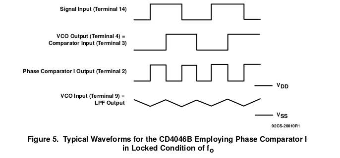
Instead of following the XOR gate logic table, type II phase detectors instead respond to rising edges of the two input signals. The following figure illustrates the concept well. Likewise, it is taken from the datasheet of Texas Instruments’ CD4046:

The longer one signal is lagging behind the other, the higher the duty cycle of the output.
One particular advantage of this phase detector is that the sign of its output depends on whether the reference frequency lags or leads the PLL’s output frequency. Furthermore, when both frequencies are equal -the PLL is locked- there is no output voltage. For these reasons the type II phase detector is also called the Phase-Frequency detector (PFD).
The Loop Filter
The loop filter’s main goal is to transform the raw output of the phase detector into something the VCO-Voltage Controlled Oscillator- can comprehend. In this case, it means transforming the phase detector’s output into a DC voltage that will be able to tune the VCO. In practice, this is usually a simple low pass filter. A simple RC filter can be enough. It eliminates the higher frequency sum product when using a type I detector, and for both types of phase detectors it smooths the output, transforming a digital square waveform into a DC voltage when using digital signals and eliminating all the parasitic harmonics.
The VCO- Voltage Controlled Oscillator
This is the building block that actually outputs our signal. Contrary to the reference oscillator, the VCO is, as the name suggests, tune-able with a control voltage. If making one from scratch (which you will most likely never do if you just want to incorporate a PLL in your designs), a common design is to use varicap diodes in a classic LC oscillator to provide tuning. More likely though, if using a PLL IC, the VCO will be a tune-able RC oscillator with some extra bells and whistles. Only at much higher frequencies will you find other topologies, such as LC oscillators.
The VCO itself doesn’t need to have a linear frequency vs. control voltage response. However, that response has to be monotonic, meaning it can only go one way: either increasing frequency with increasing voltage (definitely the most common variant), or vice-versa:
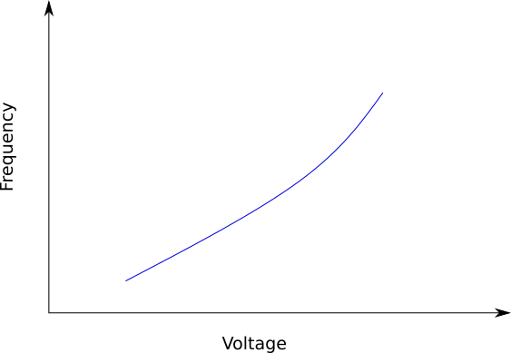
Failing to use a monotonic VCO will confuse the PLL and render it unstable and unable to lock-in.
How it All Comes Together
The phase detector takes two signals: one stable, unchanging reference signal from the reference oscillator, and one signal from the VCO, which is the PLL’s output. If the frequencies are different, the phase detector outputs a certain waveform, its duty cycle increasing the further away both signals are in terms of frequency. The loop filter then smooths out this waveform to provide a DC control voltage to the VCO, steering it into the right direction. Once both signals are at the same frequency, the DC control voltage from the loop filter stabilizes at one particular value, ensuring the VCO stays at its frequency.
You’re probably thinking to yourself that all of this, while certainly interesting, is completely useless: in this situation, the PLL’s output is exactly the same as the reference oscillator’s output. So why use a PLL at all? In this form, it’s true the PLL has no use. However, with some clever tricks we can make a tune-able oscillator with this system.
Making the PLL Tune-able
The way we are able to make a PLL tune-able is to incorporate frequency multiplication or division in either the feedback network, or after the reference oscillator:
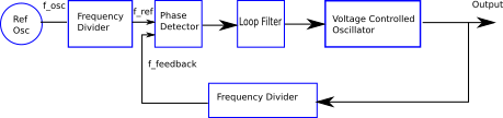
We can insert a frequency divider between the reference oscillator and the phase detector. Let this ratio be  . In this case, the reference frequency the phase detector will see is
  . Therefore, by increasing we decrease the reference frequency and thus the PLL’s output frequency.
We can also insert a frequency divider in the feedback loop, with ratio  . By increasing , the frequency the phase detector will see will decrease by a factor of . Increasing will cause the frequency after the divider to decrease. The phase detector will react accordingly and, with the loop filter, will push the VCO towards a higher frequency. Therefore, increasing increases the output frequency.
This might seem like an awkward way of creating a variable oscillator, but do keep in mind that the dividers are programmable. PLLs use a mix of analog and digital techniques to achieve their full potential. Actually changing the and ratios is very simple in practice, and is often done by a microcontroller.
By varying and , we can effectively create a tune-able oscillator with just one reference frequency. The output frequency of our PLL is:  . This method of creating an oscillator is a form of frequency synthesis. Specifically, PLLs are a form of indirect frequency synthesizers.
Designing Phase-Locked Loops
Before the advent of ICs (integrated circuits), PLLs were not considered a great solution. In discrete form, they are very finicky and complex to design and build. They were not reliable and a considerable amount of effort was required to get the circuit to work properly and consistently. This sentiment changed when PLLs became available in chip format. These ICs were cheap and could be counted on. All the hard work (well, at least most of it) was taken care of and you were left with a reliable PLL to incorporate in your designs.
There are plenty of ways to exert your creativity and ingenuity in RF design. However, I strongly suggest against designing your own PLL circuitry out of discrete components, especially if you’re a beginner. Creating each block and designing them to play nicely with each other requires a lot of testing, theory, and tweaking. If you’ve got time and passion for such a project, then of course go ahead. Designing a discrete PLL will give great insight into its inner workings. But for most of us, simply picking a reliable PLL IC to work with is the superior choice.
PLL Frequency Resolution
So now we know we can use a PLL as a variable oscillator by changing the frequency divider ratios. But by how much can we actually tune this oscillator? Unfortunately, tuning isn’t continuous, and instead occurs in steps. To illustrate this, lets take an example. Let’s suppose we have a reference frequency of 10kHz and a VCO output frequency of 10MHz, For this to work, the frequency divider would have to present 10kHz to the phase detector. To do that, the divider ration needs to be  . Now, we wish to increase the output frequency of our PLL, so we increase our divider ration by 1. We now have
  . The output frequency is still at 10MHz, but now the feedback divider presents a frequency of
  to the phase detector, which is less than the reference frequency of 10kHz. The phase-detector realizes the output frequency is too low, and together with the loop filter forces the VCO to increase its frequency. For the frequency divider to present the same 10kHz reference frequency, the VCO output needs to be
  , or 10.01MHz.
More generally, by increasing or decreasing the divider ratio by 1, we increase or decrease the PLL’s output frequency by the reference frequency presented to the phase detector. Therefore, the reference frequency is also called the PLL’s frequency resolution, or its step.
For radio communications, we need to be able to precisely tune our receiver in small steps to be able to catch a station. Steps as small as 10Hz and lower are required in the HF bands. If we are using a PLL as a frequency synthesizer, this would require us to have a very, very small reference frequency of a few Hz. Having that reference frequency isn’t a problem (we can always use a higher frequency and then use a frequency divider to achiever the necessary resolution). However, while the small reference frequency would give us excellent resolution, it also means that our loop filter would need a much lower cut-off frequency, and thus also a much lower bandwidth. At first, this might not seem like a huge deal, but filters become slower the lower the cut-off frequency is. Indeed, keep in mind the loop filter is often a simple RC filter, and in any case it will contain at least one capacitor. The lower the cut-off frequency is, the higher the value of the capacitor. The higher the capacitance, the longer it will take to actually charge it, thus delaying the filter’s response. Especially small values of cut-off frequency, such as 10Hz and lower, will cause the PLL to take a very long time to lock-in. The good news is we can get around these limitations, at the cost of a little bit of extra complexity (which is probably already built in the PLL IC anyways!).
Fractional-N PLL and Better Resolution
We know we can tune our PLL by varying the feedback divider ratio. Unfortunately, we can only tune the PLL in steps, with the frequency resolution being the reference frequency. This is true when using Integral-N PLL (the one we’ve been studying so far). However, what if we could somehow divide the output frequency by a non-integer ratio? This would allow us to tune our PLL in steps smaller than the reference frequency. This is the premise of the Fractional-N PLL. For a same frequency resolution, a fractional-N PLL will have a higher reference frequency, and thus also have a loop filter with higher cut-off frequency, which means a faster lock-time! By using a fractional-N PLL, we can get around the Integer-N PLL’s drawback of long lock-in time when using low frequency resolution.
Let’s illustrate this concept with an example. Suppose we want a tune-able oscillator with a center frequency of 10MHz and a step frequency of 10kHz. An Integer-N PLL would need a 10kHz reference frequency. A Fractional-N PLL however could get by with a 100kHz reference frequency. At 10MHz, the divider ratio would need to be 100. Increasing it by 0.1 would give us an output frequency of  . Therefore, assuming we can adjust the divider ratio down to the tenths, a 100kHz reference frequency allows for a frequency resolution of 10kHz. This only gets better the more precise we can get in our divider ratio. Being able to adjust down to the hundreds will allow a frequency resolution 100 times less than the reference frequency.
But how can we create a Fractional-N PLL? Fractional-N PLLs are nearly identical to Integer-N PLLs, save for one difference: there is an accumulator in the feedback circuit. While ideally we would be able to divide the frequency by a non-integer number in a single swoop, digital electronics prevents us from doing so. Instead, to simulate fractional frequency division, the integer feedback divider will sometimes increase or decrease its ratio by one, so that the average frequency matches what we want. Therefore, fractional-N PLLs can be thought of as dynamic integer PLLs, with their feedback divider ratio constantly changing to approximate a fractional value. The circuit responsible for adjusting the integer divider is the accumulator.
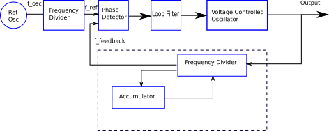
Two new variables are introduced when dealing with a fractional-N PLL:  , the fractional numerator, and
  , the fractional denominator.
  is usually determined by the IC you choose, but can sometimes be set to a certain value. is the value that you can adjust once the PLL is in operation, and can vary from 0 to
  . Thus, a fractional-N PLL’s final divider ratio is
  . Therefore the output frequency of the PLL is
  . Frequency resolution becomes
  . While the maximum can be set to will depend on the chip you are using, it can usually be set to at least 100.
Fractional-N PLL Pros and Cons
At the cost of a little extra complexity (which translates to a slightly more expensive IC chip), it seems fractional-N PLLs only provide advantages compared to thee integer-N PLL. If we are using PLLs as frequency synthesizers for use in RF designs, very low frequency steps are a requirement, and fractional-N PLLs are a necessity. However, we must be aware of a certain drawback. As explained previously, fractional-N PLLs depend on rapidly switching integer divider ratios. While this does cause the average frequency presented to the phase detector to match the required value, the instantaneous value does not. This creates spurs: unwanted noise centered around the output frequency spaced at integers or fractions of the step frequency:
Thankfully, chip manufacturers have become very good at limiting these spurs. When researching PLL chips for your own design, you might come across the term “Delta Sigma PLL”. These chips are fractional-N PLLs that use a digital modulation technique known as “Delta Sigma modulation” to greatly limit these spurs. The math and physics behind Delta Sigma modulation are outside the scope of this introductory material. Just remember that Delta Sigma Fractional-N PLLs offer the best possible performance for PLL technology today.
PLL at Higher Frequencies – the Prescaler
While theoretically we could operate a PLL in the hundreds of MHz range while keeping a low resolution, in practice there is a problem with using a very high count integer divider. The higher the output frequency and the lower the resolution, the higher the divider ratio needs to be. The maximum divider ratio depends on the amount of bits the manufacturer is willing to commit to the task. Wanting a 100MHz output with a 100Hz resolution would require, for an Integer-N PLL, a divider ratio of 1 000 000. The divider would need a counter with at least 20 bits of memory. To bring this number down to a more reasonable value, a prescaler is used. Contrary to the integer divider, the prescaler is not programmable and its dividing ratio is fixed. Having a prescaler before the divider allows the divider to do less work and thus have a lower ratio. Unfortunately, doing so also increases the step frequency. To get around this, nearly all PLL chips use what is called a dual-modulus prescaler.
This post is aimed as a refresher or for beginners, so we won’t get into the inner workings of the prescaler. When you use a PLL chip, this is transparent to the user anyways: the prescaler is usually bundled with the feedback divider anyway for higher frequency chips. I’m simply mentioning it here so you don’t get lost when you see the term “dual-modulus prescaler” in a datasheet somewhere.
Conclusion
This post ended up long than I expected it to be, but I hope it served as a helpful introduction to PLLs and how they work. Despite the lengthy article, we’ve only scratched the surface of PLL technology. For the sake of simplicity I overlooked many details, especially concerning the feedback loop and potential stability issues. My goal was to show you enough information for you to get a basic grasp on the technology and see how it could be useful in RF design. If you’d like to go more in-depth, I highly recommend taking a look at the technical documentation from Texas Instruments or Analog Devices. Here is a great first step. There will be most posts on PLLs on the future, but this time focused on their applications and how to actually interface with a PLL chip and get it working.
The two figures containing the phase detector waveforms come from a Texas Instruments Application Report, available here.